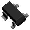
Part Details for MAX6337US23D3+T by Maxim Integrated Products
Results Overview of MAX6337US23D3+T by Maxim Integrated Products
- Distributor Offerings: (2 listings)
- Number of FFF Equivalents: (0 replacements)
- CAD Models: (Request Part)
- Number of Functional Equivalents: (0 options)
- Part Data Attributes: (Available)
- Reference Designs: (Not Available)
Tip: Data for a part may vary between manufacturers. You can filter for manufacturers on the top of the page next to the part image and part number.
MAX6337US23D3+T Information
MAX6337US23D3+T by Maxim Integrated Products is a Power Management Circuit.
Power Management Circuits are under the broader part category of Power Circuits.
A power circuit delivers electricity in order to operate a load for an electronic device. Power circuits include transformers, generators and switches. Read more about Power Circuits on our Power Circuits part category page.
Price & Stock for MAX6337US23D3+T
| Part # | Distributor | Description | Stock | Price | Buy | |
|---|---|---|---|---|---|---|
|
DISTI #
MAX6337US23D3+TCT-ND
|
DigiKey | IC SUPERVISOR 1 CHANNEL SOT143-4 Min Qty: 1 Lead time: 10 Weeks Container: Cut Tape (CT), Digi-Reel®, Tape & Reel (TR) |
10649 In Stock |
|
$2.9375 / $5.6600 | Buy Now |
|
|
Win Source Electronics | IC MPU/RESET CIRC 2.30V SOT143-4 | 1500 |
|
$2.5029 / $3.7549 | Buy Now |
Part Details for MAX6337US23D3+T
MAX6337US23D3+T CAD Models
MAX6337US23D3+T Part Data Attributes
|
|
MAX6337US23D3+T
Maxim Integrated Products
Buy Now
Datasheet
|
Compare Parts:
MAX6337US23D3+T
Maxim Integrated Products
Power Supply Support Circuit, Fixed, 1 Channel, +2.3VV, CMOS, PDSO4, LEAD FREE, TO-253, SOT-143, 4 PIN
|
| Pbfree Code | Yes | |
| Rohs Code | Yes | |
| Part Life Cycle Code | Transferred | |
| Ihs Manufacturer | MAXIM INTEGRATED PRODUCTS INC | |
| Part Package Code | SOT-143 | |
| Package Description | LEAD FREE, TO-253, SOT-143, 4 PIN | |
| Pin Count | 4 | |
| Reach Compliance Code | compliant | |
| ECCN Code | EAR99 | |
| HTS Code | 8542.39.00.01 | |
| Adjustable Threshold | NO | |
| Analog IC - Other Type | VOLTAGE SUPERVISOR/RESET IC | |
| JESD-30 Code | R-PDSO-G4 | |
| JESD-609 Code | e3 | |
| Length | 2.92 mm | |
| Moisture Sensitivity Level | 1 | |
| Number of Channels | 1 | |
| Number of Functions | 1 | |
| Number of Terminals | 4 | |
| Operating Temperature-Max | 125 °C | |
| Operating Temperature-Min | -40 °C | |
| Package Body Material | PLASTIC/EPOXY | |
| Package Code | LSOP | |
| Package Equivalence Code | TO-253 | |
| Package Shape | RECTANGULAR | |
| Package Style | SMALL OUTLINE, LOW PROFILE | |
| Peak Reflow Temperature (Cel) | 260 | |
| Qualification Status | Not Qualified | |
| Seated Height-Max | 1.22 mm | |
| Supply Current-Max (Isup) | 0.007 mA | |
| Supply Voltage-Max (Vsup) | 5.5 V | |
| Supply Voltage-Min (Vsup) | 1.2 V | |
| Supply Voltage-Nom (Vsup) | 3 V | |
| Surface Mount | YES | |
| Technology | CMOS | |
| Temperature Grade | AUTOMOTIVE | |
| Terminal Finish | MATTE TIN | |
| Terminal Form | GULL WING | |
| Terminal Pitch | 1.92 mm | |
| Terminal Position | DUAL | |
| Threshold Voltage-Nom | +2.3V | |
| Time@Peak Reflow Temperature-Max (s) | 30 | |
| Width | 1.3 mm |
MAX6337US23D3+T Frequently Asked Questions (FAQ)
-
A good PCB layout for the MAX6337US23D3+T involves keeping the input and output capacitors close to the device, using a solid ground plane, and minimizing trace lengths and widths to reduce noise and EMI.
-
To ensure stability, make sure to follow the recommended component values and PCB layout, and add a 10nF capacitor between the VOUT and ADJ pins to improve stability and reduce noise.
-
The MAX6337US23D3+T can handle input voltages up to 23V, but it's recommended to keep the input voltage below 20V to ensure reliable operation and prevent damage to the device.
-
The MAX6337US23D3+T is rated for operation up to 125°C, but it's recommended to derate the output current and voltage at high temperatures to ensure reliable operation and prevent overheating.
-
The output voltage of the MAX6337US23D3+T can be calculated using the formula: VOUT = VREF x (1 + R1/R2), where VREF is the internal reference voltage (2.5V), and R1 and R2 are the resistors connected between the VOUT and ADJ pins.
