-
Part Symbol
-
Footprint
-
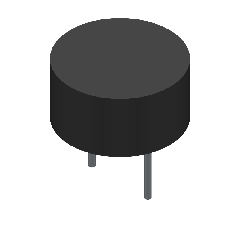
3D Model
Available Download Formats
By downloading CAD models, you agree to our Terms & Conditions and Privacy Policy
Power Field-Effect Transistor, 6.5A I(D), 100V, 0.35ohm, 1-Element, P-Channel, Silicon, Metal-oxide Semiconductor FET, TO-205AF, HERMETIC SEALED, CERAMIC, MODIFIED TO-39, 3 PIN
Tip: Data for a part may vary between manufacturers. You can filter for manufacturers on the top of the page next to the part image and part number.
JANSR2N7389 by Infineon Technologies AG is a Power Field-Effect Transistor.
Power Field-Effect Transistors are under the broader part category of Transistors.
A transistor is a small semiconductor device used to amplify, control, or create electrical signals. When selecting a transistor, factors such as voltage, current rating, gain, and power dissipation must be considered, with common types. Read more about Transistors on our Transistors part category page.
By downloading CAD models, you agree to our Terms & Conditions and Privacy Policy
|
|
JANSR2N7389
Infineon Technologies AG
Buy Now
Datasheet
|
Compare Parts:
JANSR2N7389
Infineon Technologies AG
Power Field-Effect Transistor, 6.5A I(D), 100V, 0.35ohm, 1-Element, P-Channel, Silicon, Metal-oxide Semiconductor FET, TO-205AF, HERMETIC SEALED, CERAMIC, MODIFIED TO-39, 3 PIN
|
| Rohs Code | No | |
| Part Life Cycle Code | Active | |
| Ihs Manufacturer | INFINEON TECHNOLOGIES AG | |
| Reach Compliance Code | compliant | |
| ECCN Code | EAR99 | |
| Samacsys Manufacturer | Infineon | |
| Additional Feature | HIGH RELIABILITY | |
| Avalanche Energy Rating (Eas) | 165 mJ | |
| Configuration | SINGLE WITH BUILT-IN DIODE | |
| DS Breakdown Voltage-Min | 100 V | |
| Drain Current-Max (ID) | 6.5 A | |
| Drain-source On Resistance-Max | 0.35 Ω | |
| FET Technology | METAL-OXIDE SEMICONDUCTOR | |
| JEDEC-95 Code | TO-205AF | |
| JESD-30 Code | O-CBCY-W3 | |
| JESD-609 Code | e0 | |
| Number of Elements | 1 | |
| Number of Terminals | 3 | |
| Operating Mode | ENHANCEMENT MODE | |
| Package Body Material | CERAMIC, METAL-SEALED COFIRED | |
| Package Shape | ROUND | |
| Package Style | CYLINDRICAL | |
| Polarity/Channel Type | P-CHANNEL | |
| Pulsed Drain Current-Max (IDM) | 26 A | |
| Qualification Status | Qualified | |
| Reference Standard | MIL-19500/630 | |
| Surface Mount | NO | |
| Terminal Finish | Tin/Lead (Sn/Pb) | |
| Terminal Form | WIRE | |
| Terminal Position | BOTTOM | |
| Transistor Application | SWITCHING | |
| Transistor Element Material | SILICON |
This table gives cross-reference parts and alternative options found for JANSR2N7389. The Form Fit Function (FFF) tab will give you the options that are more likely to serve as direct pin-to-pin alternates or drop-in parts. The Functional Equivalents tab will give you options that are likely to match the same function of JANSR2N7389, but it may not fit your design. Always verify details of parts you are evaluating, as these parts are offered as suggestions for what you are looking for and are not guaranteed.
| Part Number | Manufacturer | Composite Price | Description | Compare |
|---|---|---|---|---|
| IRHF93130PBF | International Rectifier | Check for Price | Power Field-Effect Transistor, 6.5A I(D), 100V, 0.35ohm, 1-Element, P-Channel, Silicon, Metal-oxide Semiconductor FET, TO-205AF, HERMETIC SEALED, CERAMIC, MODIFIED TO-39, 3 PIN | JANSR2N7389 vs IRHF93130PBF |
A 2-layer PCB with a thermal via array underneath the device is recommended. The thermal vias should be connected to a solid copper plane on the bottom layer to dissipate heat efficiently.
Ensure proper heat sinking, use a thermally conductive interface material, and follow the recommended PCB layout. Also, consider derating the device's power handling capability at high temperatures.
The JANSR2N7389 has internal ESD protection, but it's still recommended to follow standard ESD handling precautions during assembly and handling. Use an ESD wrist strap or mat, and ensure the device is stored in an anti-static bag or container.
Yes, the JANSR2N7389 is a radiation-hardened device, making it suitable for high-reliability and aerospace applications. However, ensure compliance with relevant industry standards and regulations, such as MIL-PRF-38535 or ESCC 9000.
Use a controlled soldering process with a peak temperature of 260°C (500°F) for no more than 10 seconds. Avoid using wave soldering or hot air reflow. Follow the manufacturer's recommended assembly and soldering guidelines.