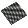
Part Details for XC7A200T-L2SBG484E by AMD Xilinx
Results Overview of XC7A200T-L2SBG484E by AMD Xilinx
- Distributor Offerings: (2 listings)
- Number of FFF Equivalents: (0 replacements)
- CAD Models: (Request Part)
- Number of Functional Equivalents: (0 options)
- Part Data Attributes: (Available)
- Reference Designs: (Not Available)
Tip: Data for a part may vary between manufacturers. You can filter for manufacturers on the top of the page next to the part image and part number.
XC7A200T-L2SBG484E Information
XC7A200T-L2SBG484E by AMD Xilinx is a Field Programmable Gate Array.
Field Programmable Gate Arrays are under the broader part category of Programmable Logic Devices.
Programmable Logic Devices (PLDs) are reconfigurable digital components that can be customized for different applications, offering flexibility and improved performance over fixed logic devices. Read more about Programmable Logic Devices on our Programmable Logic part category page.
Price & Stock for XC7A200T-L2SBG484E
| Part # | Distributor | Description | Stock | Price | Buy | |
|---|---|---|---|---|---|---|
|
|
MacroQuest Electronics | FPGA Artix-7 Family 215360 Cells 28nm Technology 1V 484-Pin FCBGA | 500 |
|
$286.5400 / $350.8600 | Buy Now |
|
|
Vyrian | Peripheral ICs | 1423 |
|
RFQ |
Part Details for XC7A200T-L2SBG484E
XC7A200T-L2SBG484E CAD Models
XC7A200T-L2SBG484E Part Data Attributes
|
|
XC7A200T-L2SBG484E
AMD Xilinx
Buy Now
Datasheet
|
Compare Parts:
XC7A200T-L2SBG484E
AMD Xilinx
Field Programmable Gate Array, 16825 CLBs, 1286MHz, 215360-Cell, CMOS, PBGA484, FBGA-484
|
| Pbfree Code | Yes | |
| Rohs Code | Yes | |
| Part Life Cycle Code | Transferred | |
| Ihs Manufacturer | XILINX INC | |
| Part Package Code | BGA | |
| Pin Count | 484 | |
| Reach Compliance Code | compliant | |
| ECCN Code | 3A991.D | |
| HTS Code | 8542.39.00.01 | |
| Factory Lead Time | 65 Weeks | |
| Additional Feature | ALSO OPERATES AT 1V SUPPLY | |
| Clock Frequency-Max | 1286 MHz | |
| Combinatorial Delay of a CLB-Max | 1.51 ns | |
| JESD-30 Code | S-PBGA-B484 | |
| JESD-609 Code | e1 | |
| Length | 19 mm | |
| Moisture Sensitivity Level | 4 | |
| Number of CLBs | 16825 | |
| Number of Inputs | 285 | |
| Number of Logic Cells | 215360 | |
| Number of Outputs | 285 | |
| Number of Terminals | 484 | |
| Operating Temperature-Max | 100 °C | |
| Operating Temperature-Min | ||
| Organization | 16825 CLBS | |
| Package Body Material | PLASTIC/EPOXY | |
| Package Code | FBGA | |
| Package Equivalence Code | BGA484,22X22,32 | |
| Package Shape | SQUARE | |
| Package Style | GRID ARRAY, FINE PITCH | |
| Peak Reflow Temperature (Cel) | 250 | |
| Programmable Logic Type | FIELD PROGRAMMABLE GATE ARRAY | |
| Qualification Status | Not Qualified | |
| Seated Height-Max | 2.44 mm | |
| Supply Voltage-Max | 0.93 V | |
| Supply Voltage-Min | 0.87 V | |
| Supply Voltage-Nom | 0.9 V | |
| Surface Mount | YES | |
| Technology | CMOS | |
| Terminal Finish | TIN SILVER COPPER | |
| Terminal Form | BALL | |
| Terminal Pitch | 0.8 mm | |
| Terminal Position | BOTTOM | |
| Time@Peak Reflow Temperature-Max (s) | 30 | |
| Width | 19 mm |
XC7A200T-L2SBG484E Frequently Asked Questions (FAQ)
-
The maximum power consumption of XC7A200T-L2SBG484E is approximately 12W, but it can vary depending on the specific application and usage.
-
To optimize power consumption, use the Xilinx Power Estimator (XPE) tool to estimate power consumption, and then apply power-saving techniques such as clock gating, voltage scaling, and dynamic voltage and frequency scaling.
-
The maximum operating frequency of XC7A200T-L2SBG484E is 500 MHz, but it can vary depending on the specific application and usage.
-
To implement a DDR3 memory interface with XC7A200T-L2SBG484E, use the Xilinx MIG (Memory Interface Generator) tool to generate a DDR3 controller, and then integrate it into your design using the Vivado Design Suite.
-
The maximum bandwidth of the PCIe interface in XC7A200T-L2SBG484E is x8 Gen3, which provides a bandwidth of up to 7880 MB/s.
