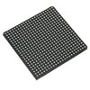
Part Details for XC6SLX75T-2FGG484I by AMD Xilinx
Results Overview of XC6SLX75T-2FGG484I by AMD Xilinx
- Distributor Offerings: (4 listings)
- Number of FFF Equivalents: (2 replacements)
- CAD Models: (Request Part)
- Number of Functional Equivalents: (10 options)
- Part Data Attributes: (Available)
- Reference Designs: (Not Available)
Tip: Data for a part may vary between manufacturers. You can filter for manufacturers on the top of the page next to the part image and part number.
XC6SLX75T-2FGG484I Information
XC6SLX75T-2FGG484I by AMD Xilinx is a Field Programmable Gate Array.
Field Programmable Gate Arrays are under the broader part category of Programmable Logic Devices.
Programmable Logic Devices (PLDs) are reconfigurable digital components that can be customized for different applications, offering flexibility and improved performance over fixed logic devices. Read more about Programmable Logic Devices on our Programmable Logic part category page.
Price & Stock for XC6SLX75T-2FGG484I
| Part # | Distributor | Description | Stock | Price | Buy | |
|---|---|---|---|---|---|---|
|
|
LCSC | FCBGA-484 Programmable Logic Device (CPLDs/FPGAs) ROHS | 100 |
|
$38.6602 / $39.8973 | Buy Now |
|
|
MacroQuest Electronics | ISO 9001: 2015, ISO 14001:2015, ISO 45001:2018 | 388 |
|
$139.2900 / $185.7200 | Buy Now |
|
|
Vyrian | Programmable ICs | 72 |
|
RFQ | |
|
|
Win Source Electronics | FPGA Spartan®-6 LXT Family 74637 Cells 45nm Technology 1.2V 484-Pin FBGA / IC FPGA 268 I/O 484FBGA | 1500 |
|
$42.3501 / $54.7021 | Buy Now |
Part Details for XC6SLX75T-2FGG484I
XC6SLX75T-2FGG484I CAD Models
XC6SLX75T-2FGG484I Part Data Attributes
|
|
XC6SLX75T-2FGG484I
AMD Xilinx
Buy Now
Datasheet
|
Compare Parts:
XC6SLX75T-2FGG484I
AMD Xilinx
Field Programmable Gate Array, 5831 CLBs, 667MHz, 74637-Cell, CMOS, PBGA484, 23 X 23 MM, 1 MM PITCH, LEAD FREE, FBGA-484
|
| Pbfree Code | Yes | |
| Rohs Code | Yes | |
| Part Life Cycle Code | Transferred | |
| Ihs Manufacturer | XILINX INC | |
| Part Package Code | BGA | |
| Package Description | 23 X 23 MM, 1 MM PITCH, LEAD FREE, FBGA-484 | |
| Pin Count | 484 | |
| Reach Compliance Code | compliant | |
| ECCN Code | 3A991.D | |
| HTS Code | 8542.39.00.01 | |
| Clock Frequency-Max | 667 MHz | |
| Combinatorial Delay of a CLB-Max | 0.26 ns | |
| JESD-30 Code | S-PBGA-B484 | |
| JESD-609 Code | e1 | |
| Length | 23 mm | |
| Moisture Sensitivity Level | 3 | |
| Number of CLBs | 5831 | |
| Number of Inputs | 268 | |
| Number of Logic Cells | 74637 | |
| Number of Outputs | 268 | |
| Number of Terminals | 484 | |
| Operating Temperature-Max | 100 °C | |
| Operating Temperature-Min | -40 °C | |
| Organization | 5831 CLBS | |
| Package Body Material | PLASTIC/EPOXY | |
| Package Code | BGA | |
| Package Equivalence Code | BGA484,22X22,40 | |
| Package Shape | SQUARE | |
| Package Style | GRID ARRAY | |
| Peak Reflow Temperature (Cel) | 250 | |
| Programmable Logic Type | FIELD PROGRAMMABLE GATE ARRAY | |
| Qualification Status | Not Qualified | |
| Seated Height-Max | 2.6 mm | |
| Supply Voltage-Max | 1.26 V | |
| Supply Voltage-Min | 1.14 V | |
| Supply Voltage-Nom | 1.2 V | |
| Surface Mount | YES | |
| Technology | CMOS | |
| Temperature Grade | INDUSTRIAL | |
| Terminal Finish | TIN SILVER COPPER | |
| Terminal Form | BALL | |
| Terminal Pitch | 1 mm | |
| Terminal Position | BOTTOM | |
| Time@Peak Reflow Temperature-Max (s) | 30 | |
| Width | 23 mm |
Alternate Parts for XC6SLX75T-2FGG484I
This table gives cross-reference parts and alternative options found for XC6SLX75T-2FGG484I. The Form Fit Function (FFF) tab will give you the options that are more likely to serve as direct pin-to-pin alternates or drop-in parts. The Functional Equivalents tab will give you options that are likely to match the same function of XC6SLX75T-2FGG484I, but it may not fit your design. Always verify details of parts you are evaluating, as these parts are offered as suggestions for what you are looking for and are not guaranteed.
| Part Number | Manufacturer | Composite Price | Description | Compare |
|---|---|---|---|---|
| XC6SLX75T-2FG484C | AMD Xilinx | Check for Price | Field Programmable Gate Array, 5831 CLBs, 667MHz, 74637-Cell, CMOS, PBGA484, 23 X 23 MM, 1 MM PITCH, FBGA-484 | XC6SLX75T-2FGG484I vs XC6SLX75T-2FG484C |
| XC6SLX75T-2FG484C | AMD | Check for Price | Field Programmable Gate Array, 5831 CLBs, 667MHz, 74637-Cell, CMOS, PBGA484, 23 X 23 MM, 1 MM PITCH, FBGA-484 | XC6SLX75T-2FGG484I vs XC6SLX75T-2FG484C |
XC6SLX75T-2FGG484I Frequently Asked Questions (FAQ)
-
The maximum power consumption of the XC6SLX75T-2FGG484I FPGA is approximately 1.5W, but this can vary depending on the specific application and usage.
-
To implement a clock domain crossing in the XC6SLX75T-2FGG484I, you can use the Xilinx-provided IP cores, such as the Clock Domain Crossing (CDC) IP, or implement a custom CDC using asynchronous FIFOs and synchronization logic.
-
The maximum frequency of the XC6SLX75T-2FGG484I FPGA's clock is 350 MHz, but this can vary depending on the specific application and usage.
-
To optimize the power consumption of the XC6SLX75T-2FGG484I FPGA, you can use power-saving features such as clock gating, voltage scaling, and dynamic voltage and frequency scaling (DVFS). Additionally, you can use Xilinx's Power Analyzer tool to identify areas of high power consumption and optimize your design accordingly.
-
The maximum bandwidth of the XC6SLX75T-2FGG484I FPGA's memory interface is 10.7 GB/s, assuming a 64-bit data bus and a clock frequency of 133 MHz.
