-
Part Symbol
-
Footprint
-
3D Model
Available Download Formats
By downloading CAD models, you agree to our Terms & Conditions and Privacy Policy

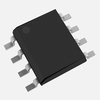
Flash, 1MX1, PDSO8, SOIC-8
Tip: Data for a part may vary between manufacturers. You can filter for manufacturers on the top of the page next to the part image and part number.
W25X10CLSNIG by Winbond Electronics Corp is a Flash Memory.
Flash Memories are under the broader part category of Memory Components.
Memory components are essential in electronics for computer processing. They can be volatile or non-volatile, depending on the desired function. Read more about Memory Components on our Memory part category page.
| Part # | Distributor | Description | Stock | Price | Buy | |
|---|---|---|---|---|---|---|
|
DISTI #
W25X10CLSNIG-ND
|
DigiKey | IC FLASH 1MBIT SPI 104MHZ 8SOIC Min Qty: 1 Lead time: 22 Weeks Container: Tube | Temporarily Out of Stock |
|
Buy Now | |
|
|
Bristol Electronics | 981 |
|
RFQ | ||
|
|
NAC | spiFlash, 1M-bit, 4Kb Uniform Sector, SOP8(150mil) Package RoHS: Compliant Package Multiple: 1 | 0 |
|
RFQ | |
|
|
Win Source Electronics | IC FLASH 1MBIT 104MHZ 8SOIC | 450000 |
|
$0.2781 / $0.4171 | Buy Now |
By downloading CAD models, you agree to our Terms & Conditions and Privacy Policy
|
|
W25X10CLSNIG
Winbond Electronics Corp
Buy Now
Datasheet
|
Compare Parts:
W25X10CLSNIG
Winbond Electronics Corp
Flash, 1MX1, PDSO8, SOIC-8
|
| Rohs Code | Yes | |
| Part Life Cycle Code | Not Recommended | |
| Ihs Manufacturer | WINBOND ELECTRONICS CORP | |
| Part Package Code | SOIC | |
| Package Description | SOIC-8 | |
| Pin Count | 8 | |
| Reach Compliance Code | compliant | |
| ECCN Code | EAR99 | |
| HTS Code | 8542.32.00.51 | |
| Samacsys Manufacturer | Winbond | |
| Additional Feature | IT ALSO OPERATES AT 2.3 V AT 80 MHZ | |
| Clock Frequency-Max (fCLK) | 104 MHz | |
| Data Retention Time-Min | 20 | |
| Endurance | 100000 Write/Erase Cycles | |
| JESD-30 Code | R-PDSO-G8 | |
| Length | 4.9 mm | |
| Memory Density | 1048576 bit | |
| Memory IC Type | FLASH | |
| Memory Width | 8 | |
| Number of Functions | 1 | |
| Number of Terminals | 8 | |
| Number of Words | 131072 words | |
| Number of Words Code | 128000 | |
| Operating Mode | SYNCHRONOUS | |
| Operating Temperature-Max | 85 °C | |
| Operating Temperature-Min | -40 °C | |
| Organization | 128KX8 | |
| Output Characteristics | 3-STATE | |
| Package Body Material | PLASTIC/EPOXY | |
| Package Code | SOP | |
| Package Equivalence Code | SOP8,.25 | |
| Package Shape | RECTANGULAR | |
| Package Style | SMALL OUTLINE | |
| Parallel/Serial | SERIAL | |
| Peak Reflow Temperature (Cel) | NOT SPECIFIED | |
| Programming Voltage | 3 V | |
| Qualification Status | Not Qualified | |
| Seated Height-Max | 1.75 mm | |
| Serial Bus Type | SPI | |
| Standby Current-Max | 0.000005 A | |
| Supply Current-Max | 0.015 mA | |
| Supply Voltage-Max (Vsup) | 3.6 V | |
| Supply Voltage-Min (Vsup) | 2.7 V | |
| Supply Voltage-Nom (Vsup) | 3 V | |
| Surface Mount | YES | |
| Technology | CMOS | |
| Temperature Grade | INDUSTRIAL | |
| Terminal Form | GULL WING | |
| Terminal Pitch | 1.27 mm | |
| Terminal Position | DUAL | |
| Time@Peak Reflow Temperature-Max (s) | NOT SPECIFIED | |
| Type | NOR TYPE | |
| Width | 3.9 mm | |
| Write Protection | HARDWARE/SOFTWARE |
The W25X10CLSNIG has a minimum of 100,000 erase cycles, but the actual number of cycles may vary depending on the usage and operating conditions.
The HOLD# signal should be kept low during a write operation to prevent any other device from accessing the flash memory. If another device tries to access the flash memory during a write operation, it may cause data corruption or other issues.
The recommended power-up sequence is to apply VCC first, followed by VPP (if used), and then the clock signal. This ensures that the device is properly initialized and ready for operation.
The optimal clock frequency depends on the specific application and system requirements. The W25X10CLSNIG can operate at frequencies up to 104 MHz, but the actual frequency used should be determined based on the system's clock speed, data transfer rate, and other factors.
The WP# pin is used to prevent accidental writes to the flash memory. When the WP# pin is low, the device is in write-protect mode, and any write operations will be ignored. When the WP# pin is high, the device is in normal operation mode, and write operations are allowed.