-
Part Symbol
-
Footprint
-
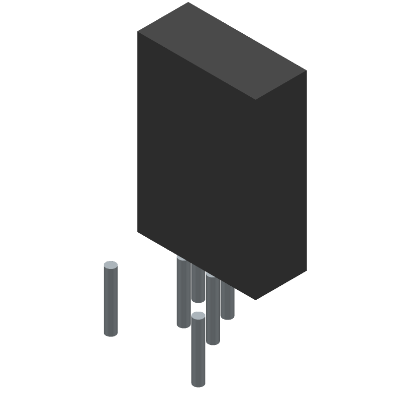
3D Model
Available Download Formats
By downloading CAD models, you agree to our Terms & Conditions and Privacy Policy

Switching Regulator, Voltage-mode, 1.44A, 140kHz Switching Freq-Max, CMOS, PZIP6, TO-262, 7/6 PIN
Tip: Data for a part may vary between manufacturers. You can filter for manufacturers on the top of the page next to the part image and part number.
TOP243FN by Power Integrations is a Switching Regulator or Controller.
Switching Regulator or Controllers are under the broader part category of Power Circuits.
A power circuit delivers electricity in order to operate a load for an electronic device. Power circuits include transformers, generators and switches. Read more about Power Circuits on our Power Circuits part category page.
| Part # | Distributor | Description | Stock | Price | Buy | |
|---|---|---|---|---|---|---|
|
|
ComSIT USA | Extended Power, Design Flexible, EcoSmart, Integrated Off-Line Switcher Switching Regulator, Voltage-mode, 1.44A, 140kHz Switching Freq-Max, CMOS, PZIP6 ECCN: EAR99 RoHS: Compliant |
|
|
RFQ |
By downloading CAD models, you agree to our Terms & Conditions and Privacy Policy
|
|
TOP243FN
Power Integrations
Buy Now
Datasheet
|
Compare Parts:
TOP243FN
Power Integrations
Switching Regulator, Voltage-mode, 1.44A, 140kHz Switching Freq-Max, CMOS, PZIP6, TO-262, 7/6 PIN
|
| Pbfree Code | Yes | |
| Rohs Code | Yes | |
| Part Life Cycle Code | Obsolete | |
| Ihs Manufacturer | POWER INTEGRATIONS INC | |
| Part Package Code | TO-262 | |
| Pin Count | 3 | |
| Reach Compliance Code | compliant | |
| ECCN Code | EAR99 | |
| HTS Code | 8542.39.00.01 | |
| Samacsys Manufacturer | Power Integrations |
The maximum operating temperature range for the TOP243FN is -40°C to 150°C, but the device is typically specified for operation up to 125°C.
To ensure reliable start-up, make sure the input voltage rises monotonically and the input voltage is above the UVLO (Under-Voltage Lockout) threshold of 12V. Also, ensure that the output voltage is not pre-biased before applying the input voltage.
For optimal performance, follow the recommended layout and PCB design guidelines provided in the application notes and evaluation board documentation. Key considerations include minimizing the loop area of the transformer and output rectifier, using a solid ground plane, and keeping the input and output stages separate.
Select a transformer with a turns ratio that matches the desired output voltage, and ensure it meets the minimum primary inductance requirement of 1.5μH. Also, consider the transformer's core material, wire gauge, and construction to ensure it can handle the required power and frequency.
To ensure EMI compliance, use a common-mode choke and X-capacitors in the input stage, and consider adding a Y-capacitor between the primary and secondary sides. Also, follow the recommended PCB layout and shielding guidelines to minimize radiated emissions.