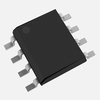
Part Details for TL431CDG by Rochester Electronics LLC
Results Overview of TL431CDG by Rochester Electronics LLC
- Distributor Offerings: (1 listing)
- Number of FFF Equivalents: (0 replacements)
- CAD Models: (Request Part)
- Number of Functional Equivalents: (2 options)
- Part Data Attributes: (Available)
- Reference Designs: (Not Available)
Tip: Data for a part may vary between manufacturers. You can filter for manufacturers on the top of the page next to the part image and part number.
TL431CDG Information
TL431CDG by Rochester Electronics LLC is a Voltage Reference.
Voltage References are under the broader part category of Power Circuits.
A power circuit delivers electricity in order to operate a load for an electronic device. Power circuits include transformers, generators and switches. Read more about Power Circuits on our Power Circuits part category page.
Price & Stock for TL431CDG
| Part # | Distributor | Description | Stock | Price | Buy | |
|---|---|---|---|---|---|---|
|
|
Vyrian | Other Function Semiconductors | 1715 |
|
RFQ |
Part Details for TL431CDG
TL431CDG CAD Models
TL431CDG Part Data Attributes
|
|
TL431CDG
Rochester Electronics LLC
Buy Now
Datasheet
|
Compare Parts:
TL431CDG
Rochester Electronics LLC
Three Terminal Voltage Reference, 1 Output, 2.495V, Trim/Adjustable, BIPolar, PDSO8, LEAD FREE, PLASTIC, SOIC-8
|
| Pbfree Code | Yes | |
| Rohs Code | Yes | |
| Part Life Cycle Code | Obsolete | |
| Ihs Manufacturer | ROCHESTER ELECTRONICS LLC | |
| Part Package Code | SOIC | |
| Package Description | LEAD FREE, PLASTIC, SOIC-8 | |
| Pin Count | 8 | |
| Reach Compliance Code | unknown | |
| ECCN Code | EAR99 | |
| HTS Code | 8542.39.00.01 | |
| Additional Feature | OUTPUT VOLTAGE PROGRAMMABLE FROM 2.495V TO 36V | |
| Analog IC - Other Type | TWO TERMINAL VOLTAGE REFERENCE | |
| JESD-30 Code | R-PDSO-G8 | |
| JESD-609 Code | e4 | |
| Length | 4.9 mm | |
| Moisture Sensitivity Level | 1 | |
| Number of Functions | 1 | |
| Number of Outputs | 1 | |
| Number of Terminals | 8 | |
| Operating Temperature-Max | 70 °C | |
| Operating Temperature-Min | ||
| Output Voltage-Max | 2.567 V | |
| Output Voltage-Min | 2.423 V | |
| Output Voltage-Nom | 2.495 V | |
| Package Body Material | PLASTIC/EPOXY | |
| Package Code | SOP | |
| Package Shape | RECTANGULAR | |
| Package Style | SMALL OUTLINE | |
| Qualification Status | Not Qualified | |
| Seated Height-Max | 1.75 mm | |
| Supply Voltage-Max (Vsup) | 36 V | |
| Supply Voltage-Min (Vsup) | 2.495 V | |
| Surface Mount | YES | |
| Technology | BIPOLAR | |
| Temp Coef of Voltage-Max | 97.338 ppm/°C | |
| Temperature Grade | COMMERCIAL | |
| Terminal Finish | NICKEL PALLADIUM GOLD | |
| Terminal Form | GULL WING | |
| Terminal Pitch | 1.27 mm | |
| Terminal Position | DUAL | |
| Trim/Adjustable Output | YES | |
| Width | 3.9 mm |
Alternate Parts for TL431CDG
This table gives cross-reference parts and alternative options found for TL431CDG. The Form Fit Function (FFF) tab will give you the options that are more likely to serve as direct pin-to-pin alternates or drop-in parts. The Functional Equivalents tab will give you options that are likely to match the same function of TL431CDG, but it may not fit your design. Always verify details of parts you are evaluating, as these parts are offered as suggestions for what you are looking for and are not guaranteed.
| Part Number | Manufacturer | Composite Price | Description | Compare |
|---|---|---|---|---|
| TL431CDG | onsemi | $0.1852 | Voltage Reference, Programmable Precision, Shunt Regulator, SOIC-8 Narrow Body, 98-TUBE | TL431CDG vs TL431CDG |
| TL431CD | STMicroelectronics | Check for Price | Programmable Voltage Reference | TL431CDG vs TL431CD |
TL431CDG Frequently Asked Questions (FAQ)
-
The recommended operating temperature range for TL431CDG is -40°C to 125°C. However, it's essential to note that the device's performance may vary outside the typical operating temperature range of 0°C to 70°C.
-
To ensure stability, it's crucial to follow the recommended layout and decoupling guidelines. Use a 0.1 μF to 1 μF ceramic capacitor between the REF and ADJ pins, and a 10 μF to 100 μF electrolytic capacitor between the VIN and GND pins. Additionally, keep the impedance of the output circuit low to prevent oscillations.
-
The maximum allowed voltage on the VIN pin is 36 V. Exceeding this voltage can damage the device. It's essential to ensure that the input voltage is within the recommended range to maintain the device's reliability and performance.
-
Yes, the TL431CDG can be used as a voltage regulator. It can be configured as a shunt regulator, where the output voltage is set by the voltage divider network between the VIN and ADJ pins. However, it's essential to note that the TL431CDG is not a traditional voltage regulator and may not provide the same level of regulation as a dedicated voltage regulator IC.
-
The output voltage of the TL431CDG can be calculated using the formula: VOUT = VREF * (1 + R1/R2), where VREF is the reference voltage (2.495 V typical), R1 is the resistance between the VIN and ADJ pins, and R2 is the resistance between the ADJ pin and GND.
