-
Part Symbol
-
Footprint
-
3D Model
Available Download Formats
By downloading CAD models, you agree to our Terms & Conditions and Privacy Policy
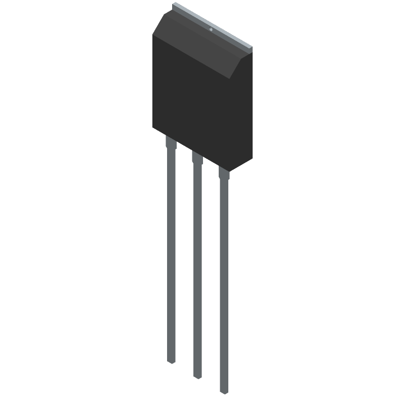
Trans MOSFET N-CH 500V 20A 3-Pin(3+Tab) TO-3PN
Tip: Data for a part may vary between manufacturers. You can filter for manufacturers on the top of the page next to the part image and part number.
TK20J50D(F) by Toshiba America Electronic Components is a Power Field-Effect Transistor.
Power Field-Effect Transistors are under the broader part category of Transistors.
A transistor is a small semiconductor device used to amplify, control, or create electrical signals. When selecting a transistor, factors such as voltage, current rating, gain, and power dissipation must be considered, with common types. Read more about Transistors on our Transistors part category page.
| Part # | Distributor | Description | Stock | Price | Buy | |
|---|---|---|---|---|---|---|
|
DISTI #
TK20J50D(F)
|
Avnet Americas | Trans MOSFET N-CH 500V 20A 3-Pin(3+Tab) TO-3PN - Bulk (Alt: TK20J50D(F)) RoHS: Compliant Min Qty: 50 Package Multiple: 50 Lead time: 16 Weeks, 0 Days Container: Bulk | 0 |
|
RFQ | |
|
DISTI #
757-TK20J50D(F)
|
Mouser Electronics | MOSFETs PD=280W VDS=500V N-Silicon N CH MOS RoHS: Compliant | 3276 |
|
$1.3000 / $3.0800 | Buy Now |
|
DISTI #
TK20J50D(F)
|
Avnet Asia | Trans MOSFET N-CH 500V 20A 3-Pin(3+Tab) TO-3PN (Alt: TK20J50D(F)) RoHS: Compliant Min Qty: 200 Package Multiple: 100 Lead time: 24 Weeks, 0 Days | 0 |
|
RFQ | |
|
DISTI #
TK20J50D(F)
|
EBV Elektronik | Trans MOSFET NCH 500V 20A 3Pin3Tab TO3PN (Alt: TK20J50D(F)) RoHS: Compliant Min Qty: 50 Package Multiple: 50 Lead time: 19 Weeks, 0 Days | EBV - 0 |
|
Buy Now |
By downloading CAD models, you agree to our Terms & Conditions and Privacy Policy
|
|
TK20J50D(F)
Toshiba America Electronic Components
Buy Now
Datasheet
|
Compare Parts:
TK20J50D(F)
Toshiba America Electronic Components
Trans MOSFET N-CH 500V 20A 3-Pin(3+Tab) TO-3PN
|
| Rohs Code | Yes | |
| Part Life Cycle Code | Active | |
| Ihs Manufacturer | TOSHIBA CORP | |
| Package Description | SC-65, 3 PIN | |
| Reach Compliance Code | compliant | |
| ECCN Code | EAR99 | |
| Factory Lead Time | 16 Weeks | |
| Samacsys Manufacturer | Toshiba | |
| Avalanche Energy Rating (Eas) | 470 mJ | |
| Case Connection | DRAIN | |
| Configuration | SINGLE WITH BUILT-IN DIODE | |
| DS Breakdown Voltage-Min | 500 V | |
| Drain Current-Max (ID) | 20 A | |
| Drain-source On Resistance-Max | 0.27 Ω | |
| FET Technology | METAL-OXIDE SEMICONDUCTOR | |
| JESD-30 Code | R-PSFM-T3 | |
| Number of Elements | 1 | |
| Number of Terminals | 3 | |
| Operating Mode | ENHANCEMENT MODE | |
| Operating Temperature-Max | 150 °C | |
| Package Body Material | PLASTIC/EPOXY | |
| Package Shape | RECTANGULAR | |
| Package Style | FLANGE MOUNT | |
| Peak Reflow Temperature (Cel) | 260 | |
| Polarity/Channel Type | N-CHANNEL | |
| Power Dissipation-Max (Abs) | 280 W | |
| Pulsed Drain Current-Max (IDM) | 80 A | |
| Surface Mount | NO | |
| Terminal Form | THROUGH-HOLE | |
| Terminal Position | SINGLE | |
| Time@Peak Reflow Temperature-Max (s) | 30 | |
| Transistor Application | SWITCHING | |
| Transistor Element Material | SILICON |
This table gives cross-reference parts and alternative options found for TK20J50D(F). The Form Fit Function (FFF) tab will give you the options that are more likely to serve as direct pin-to-pin alternates or drop-in parts. The Functional Equivalents tab will give you options that are likely to match the same function of TK20J50D(F), but it may not fit your design. Always verify details of parts you are evaluating, as these parts are offered as suggestions for what you are looking for and are not guaranteed.
| Part Number | Manufacturer | Composite Price | Description | Compare |
|---|---|---|---|---|
| TK20J50D(Q) | Toshiba America Electronic Components | Check for Price | TRANSISTOR,MOSFET,N-CHANNEL,500V V(BR)DSS,20A I(D),TO-247VAR | TK20J50D(F) vs TK20J50D(Q) |
A recommended PCB layout for optimal thermal performance would be to have a large copper area on the top and bottom layers, connected to the drain pin, to dissipate heat efficiently. Additionally, using thermal vias to connect the top and bottom layers can further improve heat dissipation.
To ensure the device is properly biased, make sure to follow the recommended biasing circuit in the datasheet. This typically involves using a voltage regulator to provide a stable voltage supply, and using resistors and capacitors to set the gate-source voltage and drain-source voltage within the recommended operating range.
To prevent damage, handle the device by the body or the pins, avoiding touching the die or the leads. Use an anti-static wrist strap or mat to prevent electrostatic discharge (ESD) damage. Store the device in an anti-static bag or tube to prevent damage during transportation and storage.
To determine the suitable heat sink for this device, consider the maximum power dissipation and the thermal resistance of the device. Choose a heat sink with a thermal resistance that is lower than the device's thermal resistance, and ensure the heat sink is properly mounted to the device using a thermal interface material.
The TK20J50D(F) meets the reliability and quality standards of Toshiba America Electronic Components, including ISO 9001 and IATF 16949. The device is also compliant with relevant industry standards, such as AEC-Q101 for automotive applications.