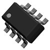
Part Details for TC1550TG-G by Supertex Inc
Results Overview of TC1550TG-G by Supertex Inc
- Distributor Offerings: (0 listings)
- Number of FFF Equivalents: (0 replacements)
- CAD Models: (Request Part)
- Number of Functional Equivalents: (0 options)
- Part Data Attributes: (Available)
- Reference Designs: (Not Available)
Tip: Data for a part may vary between manufacturers. You can filter for manufacturers on the top of the page next to the part image and part number.
TC1550TG-G Information
TC1550TG-G by Supertex Inc is a Power Field-Effect Transistor.
Power Field-Effect Transistors are under the broader part category of Transistors.
A transistor is a small semiconductor device used to amplify, control, or create electrical signals. When selecting a transistor, factors such as voltage, current rating, gain, and power dissipation must be considered, with common types. Read more about Transistors on our Transistors part category page.
Part Details for TC1550TG-G
TC1550TG-G CAD Models
TC1550TG-G Part Data Attributes
|
|
TC1550TG-G
Supertex Inc
Buy Now
Datasheet
|
Compare Parts:
TC1550TG-G
Supertex Inc
Power Field-Effect Transistor, 350A I(D), 500V, 60ohm, 2-Element, N-Channel and P-Channel, Silicon, Metal-oxide Semiconductor FET, GREEN, SO-8
|
| Pbfree Code | Yes | |
| Rohs Code | Yes | |
| Part Life Cycle Code | Transferred | |
| Ihs Manufacturer | SUPERTEX INC | |
| Part Package Code | SOT | |
| Package Description | GREEN, SO-8 | |
| Pin Count | 8 | |
| Reach Compliance Code | compliant | |
| ECCN Code | EAR99 | |
| Additional Feature | FAST SWITCHNG | |
| Configuration | SEPARATE, 2 ELEMENTS WITH BUILT-IN DIODE | |
| DS Breakdown Voltage-Min | 500 V | |
| Drain Current-Max (ID) | 350 A | |
| Drain-source On Resistance-Max | 60 Ω | |
| FET Technology | METAL-OXIDE SEMICONDUCTOR | |
| JESD-30 Code | R-PDSO-G8 | |
| JESD-609 Code | e3 | |
| Number of Elements | 2 | |
| Number of Terminals | 8 | |
| Operating Mode | ENHANCEMENT MODE | |
| Package Body Material | PLASTIC/EPOXY | |
| Package Shape | RECTANGULAR | |
| Package Style | SMALL OUTLINE | |
| Polarity/Channel Type | N-CHANNEL AND P-CHANNEL | |
| Qualification Status | Not Qualified | |
| Surface Mount | YES | |
| Terminal Finish | MATTE TIN | |
| Terminal Form | GULL WING | |
| Terminal Position | DUAL | |
| Transistor Application | AMPLIFIER | |
| Transistor Element Material | SILICON |
TC1550TG-G Frequently Asked Questions (FAQ)
-
A good PCB layout for the TC1550TG-G involves keeping the input and output traces short and separate, using a solid ground plane, and placing decoupling capacitors close to the device. A 4-layer PCB with a dedicated power plane and a separate ground plane is recommended.
-
To ensure stability, make sure to follow the recommended component values and layout guidelines. Additionally, add a 10nF to 100nF capacitor in parallel with the output resistor to prevent oscillations. Also, ensure that the input and output capacitors are of high quality and have low ESR.
-
The maximum safe operating temperature for the TC1550TG-G is 125°C. However, it's recommended to operate the device within the recommended temperature range of -40°C to 85°C for optimal performance and reliability.
-
Yes, the TC1550TG-G is suitable for high-reliability and automotive applications. It meets the requirements of AEC-Q100 Grade 1, which ensures its reliability and performance in harsh environments.
-
The output voltage ripple and noise can be calculated using the formula: ΔVout = (Iout * Rout) / (fsw * Cout), where Iout is the output current, Rout is the output resistance, fsw is the switching frequency, and Cout is the output capacitance. Additionally, consider the input voltage ripple and noise, as well as the device's internal noise and ripple specifications.
