-
Part Symbol
-
Footprint
-
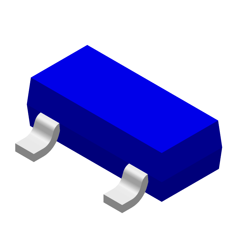
3D Model
Available Download Formats
By downloading CAD models, you agree to our Terms & Conditions and Privacy Policy
Small Signal MOS FET (Single)
Tip: Data for a part may vary between manufacturers. You can filter for manufacturers on the top of the page next to the part image and part number.
T2N7002AK by Toshiba America Electronic Components is a Small Signal Field-Effect Transistor.
Small Signal Field-Effect Transistors are under the broader part category of Transistors.
A transistor is a small semiconductor device used to amplify, control, or create electrical signals. When selecting a transistor, factors such as voltage, current rating, gain, and power dissipation must be considered, with common types. Read more about Transistors on our Transistors part category page.
| Part # | Distributor | Description | Stock | Price | Buy | |
|---|---|---|---|---|---|---|
|
|
Win Source Electronics | 281000 |
|
$0.0157 / $0.0235 | Buy Now |
By downloading CAD models, you agree to our Terms & Conditions and Privacy Policy
|
|
T2N7002AK
Toshiba America Electronic Components
Buy Now
Datasheet
|
Compare Parts:
T2N7002AK
Toshiba America Electronic Components
Small Signal MOS FET (Single)
|
| Rohs Code | Yes | |
| Part Life Cycle Code | Active | |
| Ihs Manufacturer | TOSHIBA CORP | |
| Package Description | SOT-23, 3 PIN | |
| Reach Compliance Code | compliant | |
| ECCN Code | EAR99 | |
| Factory Lead Time | 16 Weeks | |
| Samacsys Manufacturer | Toshiba | |
| Configuration | SINGLE WITH BUILT-IN DIODE AND RESISTOR | |
| DS Breakdown Voltage-Min | 60 V | |
| Drain Current-Max (ID) | 0.2 A | |
| Drain-source On Resistance-Max | 4.7 Ω | |
| FET Technology | METAL-OXIDE SEMICONDUCTOR | |
| Feedback Cap-Max (Crss) | 0.7 pF | |
| JESD-30 Code | R-PDSO-G3 | |
| Number of Elements | 1 | |
| Number of Terminals | 3 | |
| Operating Mode | ENHANCEMENT MODE | |
| Operating Temperature-Max | 150 °C | |
| Package Body Material | PLASTIC/EPOXY | |
| Package Shape | RECTANGULAR | |
| Package Style | SMALL OUTLINE | |
| Peak Reflow Temperature (Cel) | 260 | |
| Polarity/Channel Type | N-CHANNEL | |
| Power Dissipation-Max (Abs) | 1 W | |
| Surface Mount | YES | |
| Terminal Form | GULL WING | |
| Terminal Position | DUAL | |
| Time@Peak Reflow Temperature-Max (s) | 30 | |
| Transistor Application | SWITCHING | |
| Transistor Element Material | SILICON |
This table gives cross-reference parts and alternative options found for T2N7002AK. The Form Fit Function (FFF) tab will give you the options that are more likely to serve as direct pin-to-pin alternates or drop-in parts. The Functional Equivalents tab will give you options that are likely to match the same function of T2N7002AK, but it may not fit your design. Always verify details of parts you are evaluating, as these parts are offered as suggestions for what you are looking for and are not guaranteed.
| Part Number | Manufacturer | Composite Price | Description | Compare |
|---|---|---|---|---|
| SSM3K7002KF | Toshiba America Electronic Components | Check for Price | SMALL SIGNAL, FET | T2N7002AK vs SSM3K7002KF |
| SSM3K7002BFU(T5L,F) | Toshiba America Electronic Components | Check for Price | TRANSISTOR 200 mA, 60 V, N-CHANNEL, Si, SMALL SIGNAL, MOSFET, USM, 2-2E1E, SC-70, 3 PIN, FET General Purpose Small Signal | T2N7002AK vs SSM3K7002BFU(T5L,F) |
| SSM3K7002BS | Toshiba America Electronic Components | Check for Price | SMALL SIGNAL, FET | T2N7002AK vs SSM3K7002BS |
| SSM3K7002KF,LF(T | Toshiba America Electronic Components | Check for Price | Small Signal Field-Effect Transistor | T2N7002AK vs SSM3K7002KF,LF(T |
Toshiba recommends a PCB layout with a thermal pad connected to a large copper area on the bottom layer, and multiple vias to dissipate heat efficiently. A minimum of 2oz copper thickness is recommended.
The T2N7002AK requires a bias voltage of 2.5V to 5.5V on the gate pin (G) with respect to the source pin (S). A 10kΩ to 100kΩ pull-up resistor is recommended to ensure proper biasing.
The maximum allowed power dissipation for the T2N7002AK is 2.5W. Exceeding this limit may cause the device to overheat and fail.
Yes, the T2N7002AK is suitable for high-frequency switching applications up to 100kHz. However, ensure proper PCB layout and decoupling to minimize ringing and EMI.
Handle the device with ESD-safe materials and tools. Use an ESD wrist strap or mat, and ensure the device is stored in an ESD-safe package. Avoid touching the pins or leads to prevent ESD damage.