-
Part Symbol
-
Footprint
-
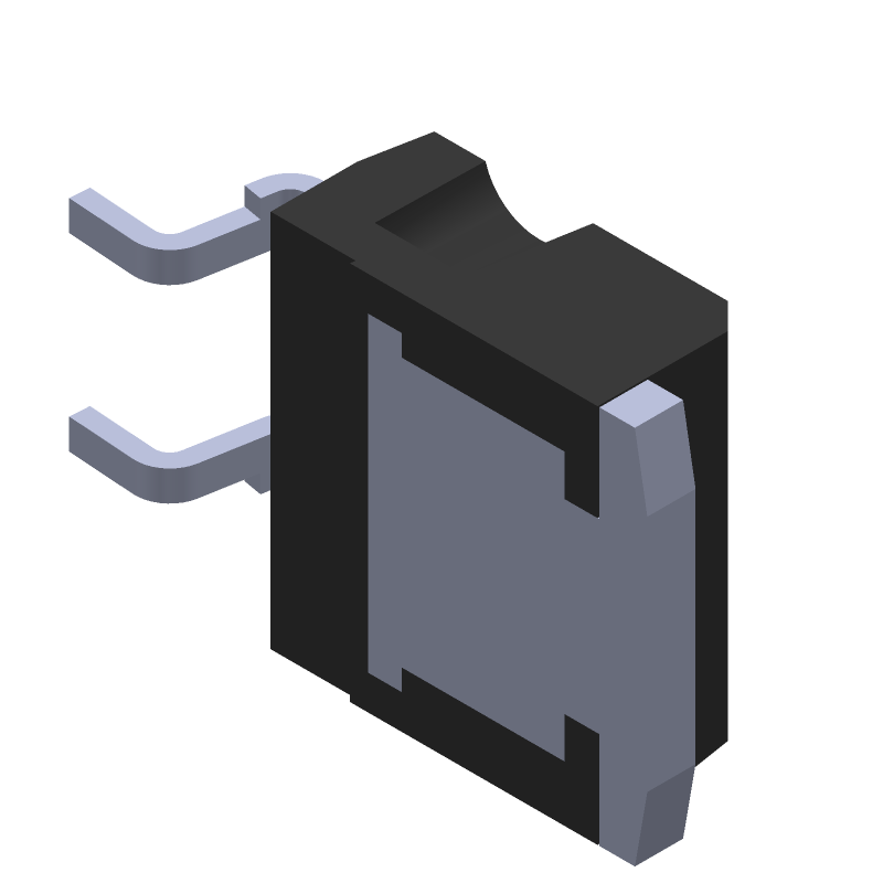
3D Model
Available Download Formats
By downloading CAD models, you agree to our Terms & Conditions and Privacy Policy
N-channel 800 V, 0.400 Ohm typ., 12 A MDmesh K5 Power MOSFET in a D2PAK package
Tip: Data for a part may vary between manufacturers. You can filter for manufacturers on the top of the page next to the part image and part number.
STB14N80K5 by STMicroelectronics is a Power Field-Effect Transistor.
Power Field-Effect Transistors are under the broader part category of Transistors.
A transistor is a small semiconductor device used to amplify, control, or create electrical signals. When selecting a transistor, factors such as voltage, current rating, gain, and power dissipation must be considered, with common types. Read more about Transistors on our Transistors part category page.
| Part # | Distributor | Description | Stock | Price | Buy | |
|---|---|---|---|---|---|---|
|
DISTI #
STB14N80K5
|
Avnet Americas | MOS Power Transistors HV (>= 200V) - Bulk (Alt: STB14N80K5) RoHS: Compliant Min Qty: 1000 Package Multiple: 1000 Lead time: 14 Weeks, 0 Days Container: Bulk | 0 |
|
$1.4496 / $1.5304 | Buy Now |
|
DISTI #
511-STB14N80K5
|
Mouser Electronics | MOSFETs N-channel 800 V, 0.400 Ohm typ 12 A MDmesh K5 Power MOSFET RoHS: Compliant | 754 |
|
$1.5100 / $4.2000 | Buy Now |
|
|
STMicroelectronics | N-channel 800 V, 0.400 Ohm typ., 12 A MDmesh K5 Power MOSFET in a D2PAK package COO: China RoHS: Compliant Min Qty: 1 | 764 |
|
$1.7200 / $4.1200 | Buy Now |
|
DISTI #
STB14N80K5
|
Avnet Silica | MOS Power Transistors HV 200V (Alt: STB14N80K5) RoHS: Compliant Min Qty: 1000 Package Multiple: 1000 Lead time: 15 Weeks, 0 Days | Silica - 1000 |
|
Buy Now | |
|
DISTI #
STB14N80K5
|
EBV Elektronik | MOS Power Transistors HV 200V (Alt: STB14N80K5) RoHS: Compliant Min Qty: 1000 Package Multiple: 1000 Lead time: 15 Weeks, 0 Days | EBV - 0 |
|
Buy Now |
By downloading CAD models, you agree to our Terms & Conditions and Privacy Policy
|
|
STB14N80K5
STMicroelectronics
Buy Now
Datasheet
|
Compare Parts:
STB14N80K5
STMicroelectronics
N-channel 800 V, 0.400 Ohm typ., 12 A MDmesh K5 Power MOSFET in a D2PAK package
|
| Rohs Code | Yes | |
| Part Life Cycle Code | Active | |
| Ihs Manufacturer | STMICROELECTRONICS | |
| Reach Compliance Code | not_compliant | |
| ECCN Code | EAR99 | |
| Factory Lead Time | 14 Weeks | |
| Samacsys Manufacturer | STMicroelectronics | |
| JESD-609 Code | e3 | |
| Moisture Sensitivity Level | 1 | |
| Peak Reflow Temperature (Cel) | 245 | |
| Terminal Finish | Matte Tin (Sn) - annealed | |
| Time@Peak Reflow Temperature-Max (s) | NOT SPECIFIED |
The maximum safe operating area (SOA) of the STB14N80K5 is not explicitly stated in the datasheet, but it can be estimated based on the device's thermal and electrical characteristics. A safe operating area can be defined as the region where the device can operate without exceeding its maximum ratings. For the STB14N80K5, this region is typically bounded by the maximum drain-source voltage (Vds), maximum drain current (Id), and maximum junction temperature (Tj). Engineers can use the device's characteristics, such as its thermal impedance and maximum power dissipation, to estimate the SOA.
To ensure the STB14N80K5 is properly biased for optimal performance, engineers should follow the recommended biasing conditions outlined in the datasheet. This typically includes setting the gate-source voltage (Vgs) within the recommended range, ensuring the drain-source voltage (Vds) is within the maximum rating, and providing a suitable gate drive circuit to minimize switching losses. Additionally, engineers should consider the device's threshold voltage (Vth) and ensure that the gate drive voltage is sufficient to fully turn on the device.
Thermal management is critical for the STB14N80K5, as excessive junction temperatures can lead to reduced performance, reliability issues, and even device failure. Engineers should consider the device's thermal impedance, maximum power dissipation, and junction-to-case thermal resistance when designing the thermal management system. This may involve using heat sinks, thermal interfaces, and forced air cooling to keep the junction temperature within the recommended range.
To minimize electromagnetic interference (EMI) when using the STB14N80K5, engineers should follow best practices for PCB design, component selection, and layout. This includes using a solid ground plane, minimizing loop areas, and keeping sensitive components away from the power stage. Additionally, engineers should consider using EMI filters, shielding, and snubbers to reduce radiated and conducted emissions.
The reliability and lifetime expectations for the STB14N80K5 are dependent on various factors, including the operating conditions, environmental factors, and manufacturing quality. Engineers can refer to the datasheet and relevant industry standards (e.g., IEC 61709) for guidance on reliability and lifetime expectations. Additionally, they should consider performing accelerated life testing and reliability analysis to estimate the device's expected lifetime under specific operating conditions.