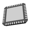
Part Details for SI5319C-C-GM by Silicon Laboratories Inc
Results Overview of SI5319C-C-GM by Silicon Laboratories Inc
- Distributor Offerings: (1 listing)
- Number of FFF Equivalents: (0 replacements)
- CAD Models: (Request Part)
- Number of Functional Equivalents: (1 option)
- Part Data Attributes: (Available)
- Reference Designs: (Not Available)
Tip: Data for a part may vary between manufacturers. You can filter for manufacturers on the top of the page next to the part image and part number.
SI5319C-C-GM Information
SI5319C-C-GM by Silicon Laboratories Inc is a Clock Generator.
Clock Generators are under the broader part category of Microcontrollers and Processors.
Microcontrollers (MCUs) are small, low-power integrated circuits used to control embedded systems. Microcontrollers are primarily used to automate and control devices. Read more about Microcontrollers and Processors on our Microcontrollers and Processors part category page.
Price & Stock for SI5319C-C-GM
| Part # | Distributor | Description | Stock | Price | Buy | |
|---|---|---|---|---|---|---|
|
|
Bristol Electronics | 18 |
|
RFQ |
Part Details for SI5319C-C-GM
SI5319C-C-GM CAD Models
SI5319C-C-GM Part Data Attributes
|
|
SI5319C-C-GM
Silicon Laboratories Inc
Buy Now
Datasheet
|
Compare Parts:
SI5319C-C-GM
Silicon Laboratories Inc
Clock Generator, 364MHz, CMOS, 6 X 6 MM, ROHS COMPLIANT, MO-220VJJD, QFN-36
|
| Rohs Code | Yes | |
| Part Life Cycle Code | Transferred | |
| Ihs Manufacturer | SILICON LABORATORIES INC | |
| Part Package Code | QFN | |
| Package Description | 6 X 6 MM, ROHS COMPLIANT, MO-220VJJD, QFN-36 | |
| Pin Count | 36 | |
| Reach Compliance Code | compliant | |
| ECCN Code | EAR99 | |
| HTS Code | 8542.39.00.01 | |
| Additional Feature | IT CAN ALSO OPERATES 2.5V OR 3.3V NON SUPPLY | |
| JESD-30 Code | S-XQCC-N36 | |
| Length | 6 mm | |
| Number of Terminals | 36 | |
| Operating Temperature-Max | 85 °C | |
| Operating Temperature-Min | -40 °C | |
| Output Clock Frequency-Max | 364 MHz | |
| Package Body Material | UNSPECIFIED | |
| Package Code | HVQCCN | |
| Package Equivalence Code | LCC36,.25SQ,20 | |
| Package Shape | SQUARE | |
| Package Style | CHIP CARRIER, HEAT SINK/SLUG, VERY THIN PROFILE | |
| Primary Clock/Crystal Frequency-Nom | 710 MHz | |
| Qualification Status | Not Qualified | |
| Seated Height-Max | 0.9 mm | |
| Supply Current-Max | 243 mA | |
| Supply Voltage-Max | 1.89 V | |
| Supply Voltage-Min | 1.71 V | |
| Supply Voltage-Nom | 1.8 V | |
| Surface Mount | YES | |
| Technology | CMOS | |
| Temperature Grade | INDUSTRIAL | |
| Terminal Form | NO LEAD | |
| Terminal Pitch | 0.5 mm | |
| Terminal Position | QUAD | |
| Width | 6 mm | |
| uPs/uCs/Peripheral ICs Type | CLOCK GENERATOR, OTHER |
Alternate Parts for SI5319C-C-GM
This table gives cross-reference parts and alternative options found for SI5319C-C-GM. The Form Fit Function (FFF) tab will give you the options that are more likely to serve as direct pin-to-pin alternates or drop-in parts. The Functional Equivalents tab will give you options that are likely to match the same function of SI5319C-C-GM, but it may not fit your design. Always verify details of parts you are evaluating, as these parts are offered as suggestions for what you are looking for and are not guaranteed.
| Part Number | Manufacturer | Composite Price | Description | Compare |
|---|---|---|---|---|
| SI5319C-C-GM | Skyworks Solutions Inc | Check for Price | Clock Generator, 364MHz, CMOS, 6 X 6 MM, ROHS COMPLIANT, MO-220VJJD, QFN-36 | SI5319C-C-GM vs SI5319C-C-GM |
SI5319C-C-GM Frequently Asked Questions (FAQ)
-
A 4-layer PCB with a solid ground plane and a separate power plane is recommended. Keep the analog and digital sections separate, and use a common mode filter on the output to reduce EMI.
-
Use a hierarchical clock tree design with a central clock source and distribute the clock signal to each component using a tree-like structure. Use a clock buffer or repeater to reduce signal degradation and ensure a clean clock signal.
-
Power up the device in the following sequence: VDD, AVDD, and then DVDD. Ensure that the power supplies are stable and within the recommended voltage range before applying the clock signal.
-
Use an oscilloscope to measure the clock signal and output signal quality. Check for signal integrity issues, such as jitter, ringing, or overshoot. Verify that the device is properly configured and that the input clock signal meets the recommended specifications.
-
The device has a maximum junction temperature of 150°C. Ensure good airflow around the device, and use a heat sink or thermal pad to dissipate heat. Reduce power consumption by optimizing the clock frequency and output load.
