-
Part Symbol
-
Footprint
-
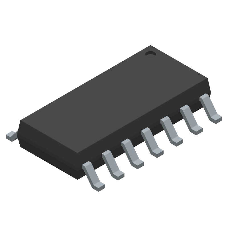
3D Model
Available Download Formats
By downloading CAD models, you agree to our Terms & Conditions and Privacy Policy
QuickSwitch 3.3V Quad Active Low Switch for Hot Swap Applications, SOIC55/Tube
Tip: Data for a part may vary between manufacturers. You can filter for manufacturers on the top of the page next to the part image and part number.
QS3VH125S1G by Renesas Electronics Corporation is a Bus Driver/Transceiver.
Bus Driver/Transceivers are under the broader part category of Logic Components.
Digital logic governs the behavior of signals in electronic circuits, enabling complex decisions based on simple binary inputs (yes/no). Logic components perform operations from these signals. Read more about Logic Components on our Logic part category page.
| Part # | Distributor | Description | Stock | Price | Buy | |
|---|---|---|---|---|---|---|
|
DISTI #
QS3VH125S1G
|
Avnet Silica | Bus Switch 4 Channel 9 Ohm 120 mA 14 Pins SOIC (Alt: QS3VH125S1G) RoHS: Compliant Min Qty: 55 Package Multiple: 55 Lead time: 143 Weeks, 0 Days | Silica - 0 |
|
Buy Now |
By downloading CAD models, you agree to our Terms & Conditions and Privacy Policy
|
|
QS3VH125S1G
Renesas Electronics Corporation
Buy Now
Datasheet
|
Compare Parts:
QS3VH125S1G
Renesas Electronics Corporation
QuickSwitch 3.3V Quad Active Low Switch for Hot Swap Applications, SOIC55/Tube
|
| Pbfree Code | Yes | |
| Rohs Code | Yes | |
| Part Life Cycle Code | Obsolete | |
| Ihs Manufacturer | RENESAS ELECTRONICS CORP | |
| Part Package Code | SOIC | |
| Pin Count | 14 | |
| Manufacturer Package Code | DCG14 | |
| Reach Compliance Code | compliant | |
| HTS Code | 8542.39.00.01 | |
| Samacsys Manufacturer | Renesas Electronics | |
| Family | CB3Q/3VH/3C/2B | |
| JESD-30 Code | R-PDSO-G14 | |
| JESD-609 Code | e3 | |
| Length | 8.65 mm | |
| Logic IC Type | BUS DRIVER | |
| Moisture Sensitivity Level | 3 | |
| Number of Bits | 1 | |
| Number of Functions | 4 | |
| Number of Ports | 2 | |
| Number of Terminals | 14 | |
| Operating Temperature-Max | 85 °C | |
| Operating Temperature-Min | -40 °C | |
| Output Characteristics | 3-STATE | |
| Output Polarity | TRUE | |
| Package Body Material | PLASTIC/EPOXY | |
| Package Code | SOP | |
| Package Equivalence Code | SOP14,.25 | |
| Package Shape | RECTANGULAR | |
| Package Style | SMALL OUTLINE | |
| Packing Method | TUBE | |
| Peak Reflow Temperature (Cel) | 260 | |
| Propagation Delay (tpd) | 0.2 ns | |
| Qualification Status | Not Qualified | |
| Seated Height-Max | 1.72 mm | |
| Supply Voltage-Max (Vsup) | 3.6 V | |
| Supply Voltage-Min (Vsup) | 2.3 V | |
| Supply Voltage-Nom (Vsup) | 2.5 V | |
| Surface Mount | YES | |
| Technology | CMOS | |
| Temperature Grade | INDUSTRIAL | |
| Terminal Finish | MATTE TIN | |
| Terminal Form | GULL WING | |
| Terminal Pitch | 1.27 mm | |
| Terminal Position | DUAL | |
| Time@Peak Reflow Temperature-Max (s) | 30 | |
| Width | 3.9 mm |
This table gives cross-reference parts and alternative options found for QS3VH125S1G. The Form Fit Function (FFF) tab will give you the options that are more likely to serve as direct pin-to-pin alternates or drop-in parts. The Functional Equivalents tab will give you options that are likely to match the same function of QS3VH125S1G, but it may not fit your design. Always verify details of parts you are evaluating, as these parts are offered as suggestions for what you are looking for and are not guaranteed.
| Part Number | Manufacturer | Composite Price | Description | Compare |
|---|---|---|---|---|
| IDTQS3VH125S1G8 | Integrated Device Technology Inc | Check for Price | Bus Driver, CB3Q/3VH/3C/2B Series, 4-Func, 1-Bit, True Output, PDSO14, SOIC-14 | QS3VH125S1G vs IDTQS3VH125S1G8 |
| IDTQS3VH125S18 | Integrated Device Technology Inc | Check for Price | Bus Driver, CB3Q/3VH/3C/2B Series, 4-Func, 1-Bit, True Output, CMOS, PDSO14, SOIC-14 | QS3VH125S1G vs IDTQS3VH125S18 |
| IDTQS3VH125S1 | Integrated Device Technology Inc | Check for Price | Bus Driver, CB3Q/3VH/3C/2B Series, 4-Func, 1-Bit, True Output, CMOS, PDSO14, SOIC-14 | QS3VH125S1G vs IDTQS3VH125S1 |
The recommended operating voltage range for the QS3VH125S1G is 1.14V to 1.26V.
To ensure signal integrity, use a low-impedance PCB design, minimize trace lengths, and use termination resistors as needed. Also, follow the recommended layout guidelines in the datasheet.
The maximum frequency of operation for the QS3VH125S1G is 125 MHz.
Power sequencing is critical when using the QS3VH125S1G. Ensure that the VCC supply is powered up before the VTT supply, and that the VCC supply is powered down after the VTT supply.
The recommended termination scheme for the QS3VH125S1G is a Thevenin termination scheme, which includes a series resistor and a parallel capacitor.