-
Part Symbol
-
Footprint
-
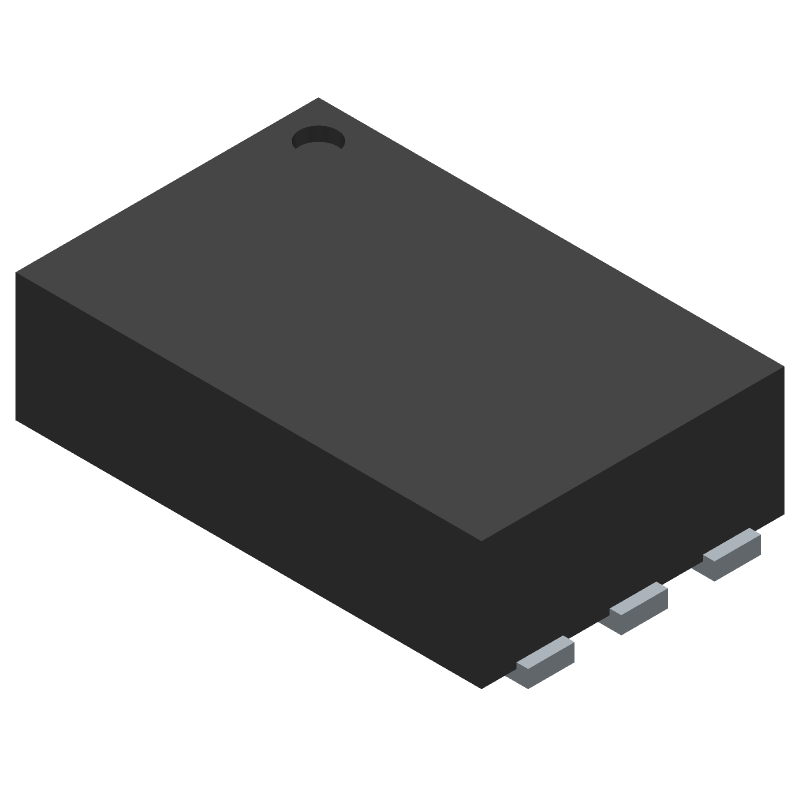
3D Model
Available Download Formats
By downloading CAD models, you agree to our Terms & Conditions and Privacy Policy
PL133 SERIES, LOW SKEW CLOCK DRIVER, 2 TRUE OUTPUT(S), 0 INVERTED OUTPUT(S), PDSO6
Tip: Data for a part may vary between manufacturers. You can filter for manufacturers on the top of the page next to the part image and part number.
PL133-27GI-R by Microchip Technology Inc is a Clock Driver.
Clock Drivers are under the broader part category of Logic Components.
Digital logic governs the behavior of signals in electronic circuits, enabling complex decisions based on simple binary inputs (yes/no). Logic components perform operations from these signals. Read more about Logic Components on our Logic part category page.
| Part # | Distributor | Description | Stock | Price | Buy | |
|---|---|---|---|---|---|---|
|
DISTI #
29AK3818
|
Newark | Fanout Buffer, 150Mhz, 3.63V, Tdfn, Clock Ic Type:Fanout Buffer, Frequency:150Mhz, No. Of Outputs:2Outputs, Supply Voltage Min:1.62V, Supply Voltage Max:3.63V, Clock Ic Case Style:Tdfn, No. Of Pins:6Pins, Product Range:- Rohs Compliant: Yes |Microchip PL133-27GI-R RoHS: Compliant Min Qty: 1 Package Multiple: 1 Date Code: 1 Container: Cut Tape | 1618 |
|
$1.2900 | Buy Now |
|
DISTI #
98Y9551
|
Newark | Industrial Grade 2-Output Dc To Mhz Cmos Buffer 6 Udfn 1.3X2.0X0.6Mm T/R Rohs Compliant: Yes |Microchip PL133-27GI-R RoHS: Compliant Min Qty: 3000 Package Multiple: 1 Date Code: 0 Container: Reel | 0 |
|
$1.5900 | Buy Now |
|
DISTI #
PL133-27GI-RCT-ND
|
DigiKey | IC CLK BUFFER 1:2 150MHZ 6DFN Min Qty: 1 Lead time: 4 Weeks Container: Digi-Reel®, Cut Tape (CT), Tape & Reel (TR) |
5326 In Stock |
|
$1.5000 / $1.9800 | Buy Now |
|
DISTI #
PL133-27GI-R
|
Avnet Americas | Clock Buffer, Fanout, 1 MHz to 150 MHz, 2 Outputs, 1.62 V to 3.63 V, 6 Pins, DFN - Tape and Reel (Alt: PL133-27GI-R) RoHS: Compliant Min Qty: 3000 Package Multiple: 3000 Lead time: 4 Weeks, 0 Days Container: Reel | 0 |
|
$1.5093 / $1.6125 | Buy Now |
|
DISTI #
998-PL133-27GI-R
|
Mouser Electronics | Clock Buffer Industrial Grade 2-Output DC to MHz CMOS Buffer RoHS: Compliant | 5345 |
|
$1.5000 / $1.9800 | Buy Now |
|
DISTI #
V36:1790_07851890
|
Arrow Electronics | Clock Fanout Buffer 2-OUT 1-IN 1:2 6-Pin DFN EP T/R RoHS: Compliant Min Qty: 3000 Package Multiple: 3000 Lead time: 4 Weeks Date Code: 2427 | Americas - 3000 |
|
$1.5420 | Buy Now |
|
DISTI #
V72:2272_07851890
|
Arrow Electronics | Clock Fanout Buffer 2-OUT 1-IN 1:2 6-Pin DFN EP T/R RoHS: Compliant Min Qty: 1 Package Multiple: 1 Lead time: 4 Weeks Date Code: 2034 Container: Cut Strips | Americas - 169 |
|
$1.7320 / $1.7940 | Buy Now |
|
DISTI #
PL133-27GI-R
|
Microchip Technology Inc | Industrial Grade 2-Output DC to MHz CMOS Buffer, UDFN, Projected EOL: 2039-10-18 COO: Thailand ECCN: EAR99 RoHS: Compliant Lead time: 10 Weeks, 0 Days Container: Reel |
0 Alternates Available |
|
$1.4400 / $1.9800 | Buy Now |
|
|
Onlinecomponents.com | Clock Fanout Buffer - 2 Out 1 In - 6-Pin DFN EP - Tape&Reel RoHS: Compliant |
2715 In Stock 15000 Factory Stock |
|
$1.4410 / $1.4710 | Buy Now |
|
DISTI #
88211702
|
Verical | Clock Fanout Buffer 2-OUT 1-IN 1:2 6-Pin DFN EP T/R RoHS: Compliant Min Qty: 3000 Package Multiple: 3000 Date Code: 2427 | Americas - 3000 |
|
$1.7951 | Buy Now |
By downloading CAD models, you agree to our Terms & Conditions and Privacy Policy
|
|
PL133-27GI-R
Microchip Technology Inc
Buy Now
Datasheet
|
Compare Parts:
PL133-27GI-R
Microchip Technology Inc
PL133 SERIES, LOW SKEW CLOCK DRIVER, 2 TRUE OUTPUT(S), 0 INVERTED OUTPUT(S), PDSO6
|
| Rohs Code | Yes | |
| Part Life Cycle Code | Active | |
| Ihs Manufacturer | MICROCHIP TECHNOLOGY INC | |
| Reach Compliance Code | compliant | |
| ECCN Code | EAR99 | |
| HTS Code | 8542.39.00.01 | |
| Factory Lead Time | 4 Weeks | |
| Samacsys Manufacturer | Microchip | |
| Family | PL133 | |
| Input Conditioning | STANDARD | |
| JESD-30 Code | R-PDSO-N6 | |
| JESD-609 Code | e4 | |
| Length | 2 mm | |
| Logic IC Type | LOW SKEW CLOCK DRIVER | |
| Number of Functions | 1 | |
| Number of Inverted Outputs | ||
| Number of Terminals | 6 | |
| Number of True Outputs | 2 | |
| Operating Temperature-Max | 85 °C | |
| Operating Temperature-Min | -40 °C | |
| Package Body Material | PLASTIC/EPOXY | |
| Package Code | HVSON | |
| Package Equivalence Code | SOLCC6,.08,16 | |
| Package Shape | RECTANGULAR | |
| Package Style | SMALL OUTLINE, HEAT SINK/SLUG, VERY THIN PROFILE | |
| Packing Method | TR | |
| Same Edge Skew-Max (tskwd) | 0.5 ns | |
| Seated Height-Max | 0.6 mm | |
| Supply Voltage-Max (Vsup) | 3.63 V | |
| Supply Voltage-Min (Vsup) | 1.62 V | |
| Supply Voltage-Nom (Vsup) | 1.8 V | |
| Surface Mount | YES | |
| Temperature Grade | INDUSTRIAL | |
| Terminal Finish | Nickel/Palladium/Gold (Ni/Pd/Au) | |
| Terminal Form | NO LEAD | |
| Terminal Pitch | 0.4 mm | |
| Terminal Position | DUAL | |
| Width | 1.3 mm |
This table gives cross-reference parts and alternative options found for PL133-27GI-R. The Form Fit Function (FFF) tab will give you the options that are more likely to serve as direct pin-to-pin alternates or drop-in parts. The Functional Equivalents tab will give you options that are likely to match the same function of PL133-27GI-R, but it may not fit your design. Always verify details of parts you are evaluating, as these parts are offered as suggestions for what you are looking for and are not guaranteed.
| Part Number | Manufacturer | Composite Price | Description | Compare |
|---|---|---|---|---|
| PL133-27GC | Microchip Technology Inc | $0.9575 | Clock Buffer Industrial Grade 2-Output DC to MHz CMOS Buffer | PL133-27GI-R vs PL133-27GC |
A 4-layer PCB with a solid ground plane and a separate power plane is recommended. Keep the signal traces short and away from the power plane to minimize noise and EMI.
Use a reliable communication protocol like SPI or I2C, and ensure proper signal termination and impedance matching. Also, implement error detection and correction mechanisms to handle data transmission errors.
The device has a maximum junction temperature of 150°C. Ensure good airflow, use a heat sink if necessary, and avoid blocking the airflow around the device. Also, follow the recommended PCB layout and thermal design guidelines.
Follow the recommended power-up and power-down sequencing in the datasheet. Use a low-dropout regulator (LDO) or a switching regulator to ensure a stable and regulated power supply to the device.
Follow proper ESD handling and storage procedures. Use ESD-protective packaging and handling equipment. Implement ESD protection circuits and devices in the system design to prevent damage from electrostatic discharge.