-
Part Symbol
-
Footprint
-
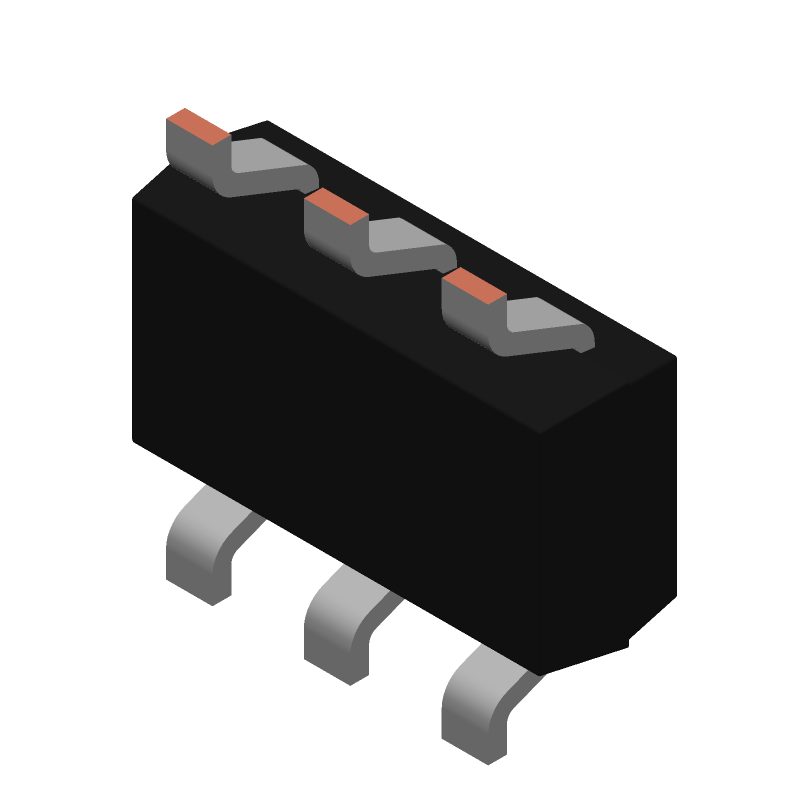
3D Model
Available Download Formats
By downloading CAD models, you agree to our Terms & Conditions and Privacy Policy
Small Signal Bipolar Transistor
Tip: Data for a part may vary between manufacturers. You can filter for manufacturers on the top of the page next to the part image and part number.
PBSS4140DPN by Nexperia is a Small Signal Bipolar Transistor.
Small Signal Bipolar Transistors are under the broader part category of Transistors.
A transistor is a small semiconductor device used to amplify, control, or create electrical signals. When selecting a transistor, factors such as voltage, current rating, gain, and power dissipation must be considered, with common types. Read more about Transistors on our Transistors part category page.
By downloading CAD models, you agree to our Terms & Conditions and Privacy Policy
|
|
PBSS4140DPN
Nexperia
Buy Now
Datasheet
|
Compare Parts:
PBSS4140DPN
Nexperia
Small Signal Bipolar Transistor
|
| Rohs Code | Yes | |
| Part Life Cycle Code | Active | |
| Ihs Manufacturer | NEXPERIA | |
| Package Description | PLASTIC, SC-74, 6 PIN | |
| Reach Compliance Code | compliant | |
| ECCN Code | EAR99 | |
| Date Of Intro | 2017-02-01 | |
| Samacsys Manufacturer | Nexperia | |
| Collector Current-Max (IC) | 1 A | |
| Collector-Emitter Voltage-Max | 40 V | |
| Configuration | SEPARATE, 2 ELEMENTS | |
| DC Current Gain-Min (hFE) | 200 | |
| JESD-30 Code | R-PDSO-G6 | |
| JESD-609 Code | e3 | |
| Moisture Sensitivity Level | 1 | |
| Number of Elements | 2 | |
| Number of Terminals | 6 | |
| Package Body Material | PLASTIC/EPOXY | |
| Package Shape | RECTANGULAR | |
| Package Style | SMALL OUTLINE | |
| Peak Reflow Temperature (Cel) | 260 | |
| Polarity/Channel Type | NPN AND PNP | |
| Surface Mount | YES | |
| Terminal Finish | TIN | |
| Terminal Form | GULL WING | |
| Terminal Position | DUAL | |
| Time@Peak Reflow Temperature-Max (s) | 30 | |
| Transistor Application | SWITCHING | |
| Transistor Element Material | SILICON | |
| Transition Frequency-Nom (fT) | 150 MHz |
The maximum operating temperature range for PBSS4140DPN is -55°C to 150°C, as specified in the datasheet. However, it's recommended to operate within -40°C to 125°C for optimal performance and reliability.
To ensure proper biasing, make sure to provide a stable voltage supply within the recommended range (VCC = 2.7 V to 5.5 V) and maintain a minimum input voltage (VIN) of 1.5 V. Additionally, ensure the input signal is within the specified frequency range (up to 100 kHz) and amplitude (up to 5 V).
For optimal thermal management, use a multi-layer PCB with a solid ground plane and ensure good thermal conductivity between the device and the PCB. Keep the device away from heat sources and use thermal vias to dissipate heat. Follow Nexperia's recommended PCB layout guidelines for the PBSS4140DPN package.
To prevent electrostatic discharge (ESD) damage, handle the device by the body or use an ESD wrist strap or mat. Ensure the PCB is designed with ESD protection in mind, using components like TVS diodes or ESD protection arrays. Follow Nexperia's ESD handling guidelines for the PBSS4140DPN.
Store the PBSS4140DPN in a dry, cool place (temperature range: -40°C to 30°C, relative humidity: 60% or less). Avoid exposing the device to direct sunlight, moisture, or extreme temperatures. Handle the device with care to prevent mechanical stress or damage.