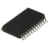
Part Details for PACVGA200Q by California Micro Devices
Results Overview of PACVGA200Q by California Micro Devices
- Distributor Offerings: (4 listings)
- Number of FFF Equivalents: (0 replacements)
- CAD Models: (Request Part)
- Number of Functional Equivalents: (0 options)
- Part Data Attributes: (Available)
- Reference Designs: (Not Available)
Tip: Data for a part may vary between manufacturers. You can filter for manufacturers on the top of the page next to the part image and part number.
Price & Stock for PACVGA200Q
| Part # | Distributor | Description | Stock | Price | Buy | |
|---|---|---|---|---|---|---|
|
|
Bristol Electronics | 5000 |
|
RFQ | ||
|
|
Quest Components | SPECIALTY CONSUMER CIRCUIT, PDSO24 | 682 |
|
$0.9775 / $2.1250 | Buy Now |
|
|
Quest Components | SPECIALTY CONSUMER CIRCUIT, PDSO24 | 617 |
|
$1.4025 / $3.4000 | Buy Now |
|
|
Velocity Electronics | Our Stock | 5000 |
|
RFQ |
Part Details for PACVGA200Q
PACVGA200Q CAD Models
PACVGA200Q Part Data Attributes
|
|
PACVGA200Q
California Micro Devices
Buy Now
Datasheet
|
Compare Parts:
PACVGA200Q
California Micro Devices
Consumer Circuit, PDSO24, QSOP-24
|
| Part Life Cycle Code | Transferred | |
| Ihs Manufacturer | CALIFORNIA MICRO DEVICES CORP | |
| Part Package Code | SOIC | |
| Package Description | QSOP-24 | |
| Pin Count | 24 | |
| Reach Compliance Code | unknown | |
| HTS Code | 8542.39.00.01 | |
| Consumer IC Type | CONSUMER CIRCUIT | |
| JESD-30 Code | R-PDSO-G24 | |
| JESD-609 Code | e0 | |
| Length | 8.65 mm | |
| Number of Functions | 1 | |
| Number of Terminals | 24 | |
| Operating Temperature-Max | 70 °C | |
| Operating Temperature-Min | ||
| Package Body Material | PLASTIC/EPOXY | |
| Package Code | SOP | |
| Package Equivalence Code | SSOP24,.24 | |
| Package Shape | RECTANGULAR | |
| Package Style | SMALL OUTLINE | |
| Qualification Status | Not Qualified | |
| Seated Height-Max | 1.75 mm | |
| Surface Mount | YES | |
| Temperature Grade | COMMERCIAL | |
| Terminal Finish | TIN LEAD | |
| Terminal Form | GULL WING | |
| Terminal Pitch | 0.635 mm | |
| Terminal Position | DUAL | |
| Width | 3.9116 mm |
PACVGA200Q Frequently Asked Questions (FAQ)
-
A good PCB layout for the PACVGA200Q involves keeping the input and output traces short and symmetrical, using a solid ground plane, and placing decoupling capacitors close to the device. A 4-layer PCB with a dedicated power plane and a separate ground plane is recommended.
-
To ensure proper biasing, make sure to connect the VCC pin to a stable 5V power supply, and the VEE pin to a stable -5V power supply. Also, ensure that the input signals are within the recommended voltage range of 0V to 3.5V.
-
The PACVGA200Q is rated for operation from -40°C to +85°C. However, it's recommended to operate the device within a temperature range of 0°C to 70°C for optimal performance and reliability.
-
Yes, the PACVGA200Q is designed for high-frequency applications up to 200 MHz. However, it's essential to follow proper PCB layout and design guidelines to minimize signal reflections and ensure optimal performance.
-
The PACVGA200Q has built-in ESD protection, but it's still recommended to follow proper ESD handling procedures during assembly and testing. Use an ESD wrist strap or mat, and ensure that the device is handled in a static-free environment.
