-
Part Symbol
-
Footprint
-
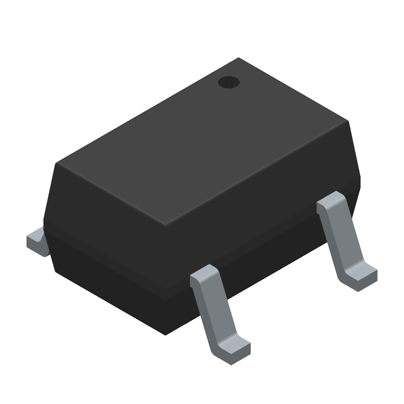
3D Model
Available Download Formats
By downloading CAD models, you agree to our Terms & Conditions and Privacy Policy

Dual NPN Bipolar Digital Transistor (BRT), SC-88A (SC-70-5 / SOT-353), 3000-REEL
Tip: Data for a part may vary between manufacturers. You can filter for manufacturers on the top of the page next to the part image and part number.
NSB1706DMW5T1G by onsemi is a Small Signal Bipolar Transistor.
Small Signal Bipolar Transistors are under the broader part category of Transistors.
A transistor is a small semiconductor device used to amplify, control, or create electrical signals. When selecting a transistor, factors such as voltage, current rating, gain, and power dissipation must be considered, with common types. Read more about Transistors on our Transistors part category page.
| Part # | Distributor | Description | Stock | Price | Buy | |
|---|---|---|---|---|---|---|
|
DISTI #
14AC4753
|
Newark | Transistor, Aec-Q101, Dual Npn, Sot-353, Digital Transistor Polarity:Dual Npn, Collector Emitter Voltage V(Br)Ceo:50V, Continuous Collector Current Ic:100Ma, Base Input Resistor R1:4.7Kohm, Base-Emitter Resistor R2:47Kohm, Resistor Rohs Compliant: Yes |Onsemi NSB1706DMW5T1G RoHS: Compliant Min Qty: 5 Package Multiple: 1 Date Code: 1 Container: Cut Tape | 2350 |
|
$0.0940 / $0.2880 | Buy Now |
|
DISTI #
88H5086
|
Newark | Brt Transistor, 50V, 47K/4.7Kohm, Sot353, Full Reel, Transistor Polarity:Dual Npn, Collector Emitter Voltage Max Npn:50V, Collector Emitter Voltage Max Pnp:-, Continuous Collector Current:100Ma, Base Input Resistor R1:4.7Kohm Rohs Compliant: Yes |Onsemi NSB1706DMW5T1G RoHS: Compliant Min Qty: 6000 Package Multiple: 1 Date Code: 0 Container: Reel | 0 |
|
$0.0410 / $0.0580 | Buy Now |
|
DISTI #
NSB1706DMW5T1GOSCT-ND
|
DigiKey | TRANS PREBIAS 2NPN 50V SC-88A Min Qty: 1 Lead time: 11 Weeks Container: Digi-Reel®, Cut Tape (CT), Tape & Reel (TR) |
15632 In Stock |
|
$0.0321 / $0.2700 | Buy Now |
|
DISTI #
NSB1706DMW5T1G
|
Avnet Americas | Bipolar Pre-Biased / Digital Transistor, Dual NPN, 50 V, 100 mA, 4.7 kohm, 47 kohm - Tape and Reel (Alt: NSB1706DMW5T1G) RoHS: Compliant Min Qty: 21000 Package Multiple: 3000 Lead time: 11 Weeks, 0 Days Container: Reel | 0 |
|
$0.0321 / $0.0343 | Buy Now |
|
DISTI #
863-NSB1706DMW5T1G
|
Mouser Electronics | Digital Transistors 100mA 50V BRT NPN RoHS: Compliant | 21230 |
|
$0.0400 / $0.2700 | Buy Now |
|
DISTI #
70467455
|
RS | ON Semi NSB1706DMW5T1G Dual NPN Bipolar Transistor, 0.1 A, 50 V, 5-Pin SC-88A Min Qty: 400 Package Multiple: 1 Container: Bulk | 0 |
|
$0.1100 / $0.1290 | RFQ |
|
|
Onlinecomponents.com | Dual NPN Bipolar Digital Transistor (BRT) RoHS: Compliant | 0 |
|
$0.0308 / $0.0367 | Buy Now |
|
|
Future Electronics | NSB Series 50 V 100 mA 4.7 kOhm NPN Dual Bias Resistor Transistor - SC-88A Min Qty: 3000 Package Multiple: 3000 |
48000 null |
|
$0.0293 / $0.0315 | Buy Now |
|
DISTI #
NSB1706DMW5T1G
|
IBS Electronics | NSB1706DMW5T1G by ONSEMI is a digital BJT with NPN/PNP polarity, 50V voltage rating, 100mA current rating, in a 5-pin SC-70 package, ideal for automotive applications, RoHS compliant. Min Qty: 3000 Package Multiple: 1 | 48000 |
|
$0.0381 / $0.0410 | Buy Now |
|
|
Chip 1 Exchange | INSTOCK | 93000 |
|
RFQ |
By downloading CAD models, you agree to our Terms & Conditions and Privacy Policy
|
|
NSB1706DMW5T1G
onsemi
Buy Now
Datasheet
|
Compare Parts:
NSB1706DMW5T1G
onsemi
Dual NPN Bipolar Digital Transistor (BRT), SC-88A (SC-70-5 / SOT-353), 3000-REEL
|
| Pbfree Code | Yes | |
| Rohs Code | Yes | |
| Part Life Cycle Code | Active | |
| Ihs Manufacturer | ONSEMI | |
| Part Package Code | SC-88A (SC-70-5 / SOT-353) | |
| Package Description | HALOGEN FREE AND ROHS COMPLIANT, CASE 419A-02, SC-88A, SC-70, 5 PIN | |
| Pin Count | 5 | |
| Manufacturer Package Code | 419A-02 | |
| Reach Compliance Code | compliant | |
| ECCN Code | EAR99 | |
| Factory Lead Time | 11 Weeks | |
| Samacsys Description | Simplifies Circuit Design; Reduces Board Space; Pb-Free Package is Available; NSV Prefix for Automotive and Other Applications Requiring Unique Site and Control Change Requirements; AECQ101 Qualified and PPAP Capable | |
| Samacsys Manufacturer | onsemi | |
| Samacsys Modified On | 2025-01-22 16:53:39 | |
| Total Weight | 6.2 | |
| Category CO2 Kg | 8.8 | |
| CO2 | 54.56000000000001 | |
| EU RoHS Version | RoHS 2 (2015/863/EU) | |
| Candidate List Date | 2025-01-21 | |
| CAS Accounted for Wt | 100 | |
| EFUP | e | |
| Conflict Mineral Status | DRC Conflict Free | |
| Conflict Mineral Status Source | CMRT V6.40 | |
| Additional Feature | BUILT-IN BIAS RESISTOR | |
| Collector Current-Max (IC) | 0.1 A | |
| Collector-Emitter Voltage-Max | 50 V | |
| Configuration | COMMON EMITTER, 2 ELEMENTS WITH BUILT-IN RESISTOR | |
| DC Current Gain-Min (hFE) | 80 | |
| JESD-30 Code | R-PDSO-G5 | |
| JESD-609 Code | e3 | |
| Moisture Sensitivity Level | 1 | |
| Number of Elements | 2 | |
| Number of Terminals | 5 | |
| Operating Temperature-Max | 150 °C | |
| Package Body Material | PLASTIC/EPOXY | |
| Package Shape | RECTANGULAR | |
| Package Style | SMALL OUTLINE | |
| Peak Reflow Temperature (Cel) | 260 | |
| Polarity/Channel Type | NPN | |
| Power Dissipation-Max (Abs) | 0.385 W | |
| Qualification Status | Not Qualified | |
| Surface Mount | YES | |
| Terminal Finish | Matte Tin (Sn) - annealed | |
| Terminal Form | GULL WING | |
| Terminal Position | DUAL | |
| Time@Peak Reflow Temperature-Max (s) | 30 | |
| Transistor Application | SWITCHING | |
| Transistor Element Material | SILICON |
A 2-layer or 4-layer PCB with a solid ground plane and thermal vias is recommended. The device should be placed near a thermal pad or heat sink to dissipate heat efficiently.
Ensure proper thermal design, use a heat sink if necessary, and follow the recommended operating conditions. Also, consider using a thermal interface material (TIM) to improve heat transfer between the device and heat sink.
The maximum allowed voltage on the input pins is 5.5V, which is the absolute maximum rating. However, it's recommended to keep the input voltage within the recommended operating range of 3.0V to 5.0V for optimal performance.
Use ESD protection devices such as TVS diodes or ESD arrays on the input lines to protect the device from electrostatic discharge. Follow proper PCB design and handling practices to minimize ESD risks.
Power up the device in the following sequence: VCC, then VIN, and finally the input signals. This ensures proper device initialization and prevents latch-up or other issues.