-
Part Symbol
-
Footprint
-
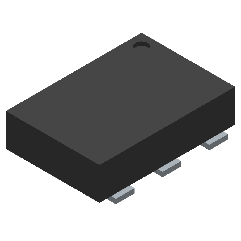
3D Model
Available Download Formats
By downloading CAD models, you agree to our Terms & Conditions and Privacy Policy

Dual Buffer with Schmitt Trigger Output, ULLGA6 1.45x1.0, 0.50P, 3000-REEL
Tip: Data for a part may vary between manufacturers. You can filter for manufacturers on the top of the page next to the part image and part number.
NLX2G17AMX1TCG by onsemi is a Gate.
Gates are under the broader part category of Logic Components.
Digital logic governs the behavior of signals in electronic circuits, enabling complex decisions based on simple binary inputs (yes/no). Logic components perform operations from these signals. Read more about Logic Components on our Logic part category page.
| Part # | Distributor | Description | Stock | Price | Buy | |
|---|---|---|---|---|---|---|
|
DISTI #
NLX2G17AMX1TCG
|
Avnet Americas | Schmitt Trigger Buffer, Non Inverting, Dual, 1 Input, 6 Pins, ULLGA, NLX2G17 - Tape and Reel (Alt: NLX2G17AMX1TCG) RoHS: Compliant Min Qty: 8334 Package Multiple: 1 Lead time: 0 Weeks, 2 Days Container: Reel | 0 |
|
$0.0770 / $0.0786 | Buy Now |
|
|
Rochester Electronics | NLX2G17 - Dual Buffer with Schmitt Trigger Output RoHS: Compliant Status: Obsolete Min Qty: 1 | 810 |
|
$0.0672 / $0.1084 | Buy Now |
|
DISTI #
NLX2G17AMX1TCG
|
TME | IC: digital, buffer,non-inverting, Ch: 2, SMD, ULLGA6, 1.65÷5.5VDC Min Qty: 3 | 0 |
|
$0.0980 / $0.2430 | RFQ |
|
DISTI #
NLX2G17AMX1TCG
|
Avnet Silica | Schmitt Trigger Buffer Non Inverting Dual 1 Input 6 Pins ULLGA NLX2G17 (Alt: NLX2G17AMX1TCG) RoHS: Compliant Min Qty: 3000 Package Multiple: 3000 Lead time: 143 Weeks, 0 Days | Silica - 0 |
|
Buy Now | |
|
DISTI #
NLX2G17AMX1TCG
|
EBV Elektronik | Schmitt Trigger Buffer Non Inverting Dual 1 Input 6 Pins ULLGA NLX2G17 (Alt: NLX2G17AMX1TCG) RoHS: Compliant Min Qty: 3000 Package Multiple: 3000 Lead time: 143 Weeks, 0 Days | EBV - 0 |
|
Buy Now | |
|
|
Flip Electronics | Stock, ship today | 21000 |
|
RFQ |
By downloading CAD models, you agree to our Terms & Conditions and Privacy Policy
|
|
NLX2G17AMX1TCG
onsemi
Buy Now
Datasheet
|
Compare Parts:
NLX2G17AMX1TCG
onsemi
Dual Buffer with Schmitt Trigger Output, ULLGA6 1.45x1.0, 0.50P, 3000-REEL
|
| Pbfree Code | Yes | |
| Rohs Code | Yes | |
| Part Life Cycle Code | Obsolete | |
| Ihs Manufacturer | ONSEMI | |
| Part Package Code | LGA | |
| Package Description | 1.45 X 1 MM, 0.50 MM PITCH, LEAD FREE, ULLGA-6 | |
| Pin Count | 6 | |
| Manufacturer Package Code | 613AF | |
| Reach Compliance Code | compliant | |
| HTS Code | 8542.39.00.01 | |
| Factory Lead Time | 2 Days | |
| Samacsys Manufacturer | onsemi | |
| Family | 2G | |
| JESD-30 Code | R-XDSO-N6 | |
| JESD-609 Code | e4 | |
| Length | 1.45 mm | |
| Load Capacitance (CL) | 15 pF | |
| Logic IC Type | BUFFER | |
| Max I(ol) | 0.004 A | |
| Moisture Sensitivity Level | 1 | |
| Number of Functions | 2 | |
| Number of Inputs | 1 | |
| Number of Terminals | 6 | |
| Operating Temperature-Max | 125 °C | |
| Operating Temperature-Min | -55 °C | |
| Package Body Material | UNSPECIFIED | |
| Package Code | VSON | |
| Package Equivalence Code | SOLCC6,.04,14 | |
| Package Shape | RECTANGULAR | |
| Package Style | SMALL OUTLINE, VERY THIN PROFILE | |
| Packing Method | TR | |
| Peak Reflow Temperature (Cel) | 260 | |
| Prop. Delay@Nom-Sup | 13 ns | |
| Propagation Delay (tpd) | 15.6 ns | |
| Qualification Status | Not Qualified | |
| Schmitt Trigger | YES | |
| Seated Height-Max | 0.4 mm | |
| Supply Voltage-Max (Vsup) | 5.5 V | |
| Supply Voltage-Min (Vsup) | 1.65 V | |
| Supply Voltage-Nom (Vsup) | 1.8 V | |
| Surface Mount | YES | |
| Technology | CMOS | |
| Temperature Grade | MILITARY | |
| Terminal Finish | NICKEL PALLADIUM GOLD | |
| Terminal Form | NO LEAD | |
| Terminal Pitch | 0.5 mm | |
| Terminal Position | DUAL | |
| Time@Peak Reflow Temperature-Max (s) | 30 | |
| Width | 1 mm |
This table gives cross-reference parts and alternative options found for NLX2G17AMX1TCG. The Form Fit Function (FFF) tab will give you the options that are more likely to serve as direct pin-to-pin alternates or drop-in parts. The Functional Equivalents tab will give you options that are likely to match the same function of NLX2G17AMX1TCG, but it may not fit your design. Always verify details of parts you are evaluating, as these parts are offered as suggestions for what you are looking for and are not guaranteed.
| Part Number | Manufacturer | Composite Price | Description | Compare |
|---|---|---|---|---|
| NLU2G17CMX1TCG | onsemi | Check for Price | Dual Buffer with Schmitt Trigger Output, ULLGA6 1.0x1.0, 0.35P, 3000-REEL | NLX2G17AMX1TCG vs NLU2G17CMX1TCG |
| MC74VHC2G17MU3TCG | onsemi | Check for Price | Dual Buffer, Schmitt Trigger Input, UDFN-6, 3000-REEL | NLX2G17AMX1TCG vs MC74VHC2G17MU3TCG |
| NLU2G17CMUTCG | onsemi | Check for Price | Dual Buffer with Schmitt Trigger Output, UDFN6 1x1 0.35P, 3000-REEL | NLX2G17AMX1TCG vs NLU2G17CMUTCG |
A 2-layer or 4-layer PCB with a solid ground plane and thermal vias is recommended. The device should be placed near a thermal pad or heat sink to dissipate heat efficiently.
Ensure that the device is operated within the recommended voltage and current limits, and that the PCB is designed to minimize thermal resistance. Also, consider using a thermal interface material (TIM) to improve heat transfer between the device and heat sink.
Exceeding the maximum TJ rating can lead to reduced device lifespan, increased thermal resistance, and potentially catastrophic failure. It is essential to ensure that the device operates within the recommended temperature range to maintain reliability.
Use ESD protection devices such as TVS diodes or ESD arrays on the input and output pins to protect against electrostatic discharge. Also, ensure that the PCB is designed with ESD protection in mind, including the use of ESD-resistant components and connectors.
Use a soldering temperature of 260°C (500°F) for a maximum of 10 seconds. Ensure that the soldering process is done in a nitrogen atmosphere to prevent oxidation. Follow the recommended soldering profile to prevent damage to the device.