-
Part Symbol
-
Footprint
-
3D Model
Available Download Formats
By downloading CAD models, you agree to our Terms & Conditions and Privacy Policy
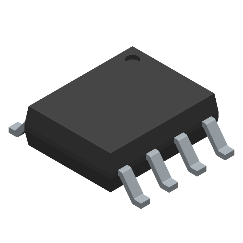
Single P-Channel Enhancement Mode Field Effect Transistor -20V, -6.5A, 35mΩ, SOIC-8, 2500-REEL
Tip: Data for a part may vary between manufacturers. You can filter for manufacturers on the top of the page next to the part image and part number.
NDS8434 by onsemi is a Small Signal Field-Effect Transistor.
Small Signal Field-Effect Transistors are under the broader part category of Transistors.
A transistor is a small semiconductor device used to amplify, control, or create electrical signals. When selecting a transistor, factors such as voltage, current rating, gain, and power dissipation must be considered, with common types. Read more about Transistors on our Transistors part category page.
| Part # | Distributor | Description | Stock | Price | Buy | |
|---|---|---|---|---|---|---|
|
DISTI #
31Y3204
|
Newark | Mosfet, P-Ch, -20V, -6.5A, Soic-8, Channel Type:P Channel, Drain Source Voltage Vds:20V, Continuous Drain Current Id:6.5A, Transistor Mounting:Surface Mount, Rds(On) Test Voltage:4.5V, Gate Source Threshold Voltage Max:700Mv Rohs Compliant: Yes |Onsemi NDS8434 RoHS: Compliant Min Qty: 1 Package Multiple: 1 Date Code: 0 Container: Cut Tape | 0 |
|
Buy Now | |
|
DISTI #
NDS8434
|
Avnet Americas | Trans MOSFET P-CH 20V 6.5A 8-Pin SOIC N T/R - Tape and Reel (Alt: NDS8434) RoHS: Compliant Min Qty: 1064 Package Multiple: 1 Lead time: 0 Weeks, 2 Days Container: Reel | 5167 Partner Stock |
|
$0.6572 / $0.6709 | Buy Now |
|
DISTI #
86006603
|
Verical | Trans MOSFET P-CH 20V 6.5A 8-Pin SOIC T/R RoHS: Compliant Min Qty: 325 Package Multiple: 1 Date Code: 2101 | Americas - 635 |
|
$0.7170 / $1.1565 | Buy Now |
|
|
Quest Components | 6500 MA, 20 V, P-CHANNEL, SI, SMALL SIGNAL, MOSFET | 20 |
|
$0.5940 / $0.9900 | Buy Now |
|
|
Rochester Electronics | NDS8434 - Small Signal Field-Effect Transistor, 6.5A, 20V, P-Channel, MOSFET RoHS: Compliant Status: Obsolete Min Qty: 1 | 635 |
|
$0.5736 / $0.9252 | Buy Now |
|
DISTI #
NDS8434
|
Avnet Silica | Trans MOSFET PCH 20V 65A 8Pin SOIC N TR (Alt: NDS8434) RoHS: Compliant Min Qty: 2500 Package Multiple: 2500 Lead time: 143 Weeks, 0 Days | Silica - 0 |
|
Buy Now | |
|
DISTI #
NDS8434
|
EBV Elektronik | Trans MOSFET PCH 20V 65A 8Pin SOIC N TR (Alt: NDS8434) RoHS: Compliant Min Qty: 2500 Package Multiple: 2500 Lead time: 143 Weeks, 0 Days | EBV - 0 |
|
Buy Now | |
|
|
Flip Electronics | Stock, ship today | 5167 |
|
RFQ |
By downloading CAD models, you agree to our Terms & Conditions and Privacy Policy
|
|
NDS8434
onsemi
Buy Now
Datasheet
|
Compare Parts:
NDS8434
onsemi
Single P-Channel Enhancement Mode Field Effect Transistor -20V, -6.5A, 35mΩ, SOIC-8, 2500-REEL
|
| Pbfree Code | Yes | |
| Rohs Code | Yes | |
| Part Life Cycle Code | Obsolete | |
| Ihs Manufacturer | ONSEMI | |
| Part Package Code | SOIC-8 | |
| Package Description | SOIC-8 | |
| Manufacturer Package Code | 751EB | |
| Reach Compliance Code | compliant | |
| ECCN Code | EAR99 | |
| Factory Lead Time | 2 Days | |
| Samacsys Manufacturer | onsemi | |
| Configuration | SINGLE WITH BUILT-IN DIODE | |
| DS Breakdown Voltage-Min | 20 V | |
| Drain Current-Max (ID) | 6.5 A | |
| Drain-source On Resistance-Max | 0.035 Ω | |
| FET Technology | METAL-OXIDE SEMICONDUCTOR | |
| JESD-30 Code | R-PDSO-G8 | |
| JESD-609 Code | e3 | |
| Moisture Sensitivity Level | 1 | |
| Number of Elements | 1 | |
| Number of Terminals | 8 | |
| Operating Mode | ENHANCEMENT MODE | |
| Operating Temperature-Max | 150 °C | |
| Package Body Material | PLASTIC/EPOXY | |
| Package Shape | RECTANGULAR | |
| Package Style | SMALL OUTLINE | |
| Peak Reflow Temperature (Cel) | 260 | |
| Polarity/Channel Type | P-CHANNEL | |
| Power Dissipation-Max (Abs) | 1 W | |
| Qualification Status | Not Qualified | |
| Surface Mount | YES | |
| Terminal Finish | MATTE TIN | |
| Terminal Form | GULL WING | |
| Terminal Position | DUAL | |
| Time@Peak Reflow Temperature-Max (s) | 30 | |
| Transistor Application | SWITCHING | |
| Transistor Element Material | SILICON |
A 2-layer or 4-layer PCB with a solid ground plane and thermal vias is recommended. Ensure a minimum of 1 oz copper thickness and a thermal relief pattern under the device.
Implement a robust thermal management system, including a heat sink, thermal interface material, and a cooling fan if necessary. Monitor junction temperature and adjust the system design accordingly.
Focus on minimizing parasitic inductance, using a common-mode choke, and adding EMI filters. Ensure proper PCB layout, decoupling, and shielding to reduce radiated emissions.
Use a dedicated gate driver IC, ensure a low-impedance gate drive circuit, and optimize the gate resistance and capacitance for minimal power loss and EMI.
Ensure identical devices, matching thermal performance, and synchronized gate drive signals. Implement a master-slave configuration, and consider using a current-sharing bus to balance current distribution.