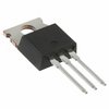
Part Details for NDF08N60ZG by onsemi
Results Overview of NDF08N60ZG by onsemi
- Distributor Offerings: (4 listings)
- Number of FFF Equivalents: (0 replacements)
- CAD Models: (Request Part)
- Number of Functional Equivalents: (0 options)
- Part Data Attributes: (Available)
- Reference Designs: (Not Available)
Tip: Data for a part may vary between manufacturers. You can filter for manufacturers on the top of the page next to the part image and part number.
NDF08N60ZG Information
NDF08N60ZG by onsemi is a Power Field-Effect Transistor.
Power Field-Effect Transistors are under the broader part category of Transistors.
A transistor is a small semiconductor device used to amplify, control, or create electrical signals. When selecting a transistor, factors such as voltage, current rating, gain, and power dissipation must be considered, with common types. Read more about Transistors on our Transistors part category page.
Price & Stock for NDF08N60ZG
| Part # | Distributor | Description | Stock | Price | Buy | |
|---|---|---|---|---|---|---|
|
DISTI #
86122575
|
Verical | Trans MOSFET N-CH 600V 8.4A 3-Pin(3+Tab) TO-220FP Tube Min Qty: 446 Package Multiple: 1 Date Code: 1401 | Americas - 53550 |
|
$0.6231 / $0.8421 | Buy Now |
|
DISTI #
86140296
|
Verical | Trans MOSFET N-CH 600V 8.4A 3-Pin(3+Tab) TO-220FP Tube Min Qty: 446 Package Multiple: 1 Date Code: 1001 | Americas - 1116 |
|
$0.6990 / $0.8421 | Buy Now |
|
DISTI #
88044319
|
Verical | Trans MOSFET N-CH 600V 8.4A 3-Pin(3+Tab) TO-220FP Tube Min Qty: 446 Package Multiple: 1 Date Code: 1101 | Americas - 600 |
|
$0.7579 / $0.8421 | Buy Now |
|
|
Rochester Electronics | 8.4A, 600V, 0.95ohm, N-Channel Power MOSFET, TO-220AB RoHS: Compliant Status: Obsolete Min Qty: 1 | 55666 |
|
$0.4177 / $0.6737 | Buy Now |
Part Details for NDF08N60ZG
NDF08N60ZG CAD Models
NDF08N60ZG Part Data Attributes
|
|
NDF08N60ZG
onsemi
Buy Now
Datasheet
|
Compare Parts:
NDF08N60ZG
onsemi
Power MOSFET 600V 7.5A 0.95 Ohm Single N-Channel TO-220FP, TO-220 3 LEAD FULLPAK, 50-TUBE
|
| Pbfree Code | Yes | |
| Rohs Code | Yes | |
| Part Life Cycle Code | Obsolete | |
| Ihs Manufacturer | ONSEMI | |
| Part Package Code | TO-220AB | |
| Pin Count | 3 | |
| Manufacturer Package Code | 221AH | |
| Reach Compliance Code | not_compliant | |
| ECCN Code | EAR99 | |
| Factory Lead Time | 4 Weeks | |
| Avalanche Energy Rating (Eas) | 235 mJ | |
| Case Connection | ISOLATED | |
| Configuration | SINGLE WITH BUILT-IN DIODE | |
| DS Breakdown Voltage-Min | 600 V | |
| Drain Current-Max (ID) | 8.4 A | |
| Drain-source On Resistance-Max | 0.95 Ω | |
| FET Technology | METAL-OXIDE SEMICONDUCTOR | |
| JEDEC-95 Code | TO-220AB | |
| JESD-30 Code | R-PSFM-T3 | |
| JESD-609 Code | e3 | |
| Number of Elements | 1 | |
| Number of Terminals | 3 | |
| Operating Mode | ENHANCEMENT MODE | |
| Operating Temperature-Max | 150 °C | |
| Package Body Material | PLASTIC/EPOXY | |
| Package Shape | RECTANGULAR | |
| Package Style | FLANGE MOUNT | |
| Polarity/Channel Type | N-CHANNEL | |
| Power Dissipation-Max (Abs) | 36 W | |
| Pulsed Drain Current-Max (IDM) | 30 A | |
| Qualification Status | Not Qualified | |
| Surface Mount | NO | |
| Terminal Finish | TIN | |
| Terminal Form | THROUGH-HOLE | |
| Terminal Position | SINGLE | |
| Transistor Element Material | SILICON |
NDF08N60ZG Frequently Asked Questions (FAQ)
-
The maximum SOA for the NDF08N60ZG is not explicitly stated in the datasheet, but it can be estimated based on the device's thermal and electrical characteristics. A safe operating area can be determined by considering the device's voltage and current ratings, as well as its thermal impedance and maximum junction temperature.
-
To ensure proper cooling, consider the device's thermal impedance, maximum junction temperature, and power dissipation. Use a heat sink with a sufficient thermal conductivity, and ensure good thermal contact between the device and heat sink. Additionally, consider using a thermal interface material and ensuring good airflow around the heat sink.
-
The recommended gate drive voltage for the NDF08N60ZG is typically between 10V and 15V, depending on the specific application and switching frequency. A higher gate drive voltage can reduce switching losses, but may also increase gate charge and power consumption.
-
To minimize EMI, use proper PCB layout techniques, such as separating high-frequency and low-frequency circuits, using ground planes, and minimizing loop areas. Additionally, consider using EMI filters, shielding, and snubbers to reduce electromagnetic radiation.
-
The maximum allowed dv/dt for the NDF08N60ZG is not explicitly stated in the datasheet, but it is typically in the range of 1-10 kV/μs. Exceeding this limit can cause the device to malfunction or fail. To ensure reliable operation, consider using a gate driver with a controlled dv/dt and a suitable snubber circuit.
