-
Part Symbol
-
Footprint
-
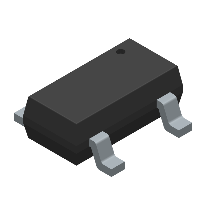
3D Model
Available Download Formats
By downloading CAD models, you agree to our Terms & Conditions and Privacy Policy

Operational Amplifier, Low bias current, Rail to Rail CMOS Op-Amp Pinout Style: 1, TSOP-5, 3000-REEL
Tip: Data for a part may vary between manufacturers. You can filter for manufacturers on the top of the page next to the part image and part number.
NCS7101SN1T1G by onsemi is an Operational Amplifier.
Operational Amplifiers are under the broader part category of Amplifier Circuits.
Amplifier circuits use external power to increase the amplitude of an input signal. They can be used to perform linear amplifications or logarithmic functions. Read more about Amplifier Circuits on our Amplifier Circuits part category page.
| Part # | Distributor | Description | Stock | Price | Buy | |
|---|---|---|---|---|---|---|
|
DISTI #
83H7675
|
Newark | Ic, operational Amplifier, single, cmos, tsop,5Pin, plastic Rohs Compliant: Yes |Onsemi NCS7101SN1T1G RoHS: Compliant Min Qty: 3000 Package Multiple: 1 Date Code: 0 Container: Reel | 0 |
|
$0.3040 / $0.3950 | Buy Now |
|
DISTI #
NCS7101SN1T1GOSCT-ND
|
DigiKey | IC OPAMP GP 1 CIRCUIT 5TSOP Min Qty: 1 Lead time: 9 Weeks Container: Cut Tape (CT), Digi-Reel®, Tape & Reel (TR) |
13326 In Stock |
|
$0.2938 / $1.4000 | Buy Now |
|
DISTI #
NCS7101SN1T1G
|
Avnet Americas | OP Amp Single GP R-R I/O ?5V/10V 5-Pin TSOP T/R - Tape and Reel (Alt: NCS7101SN1T1G) RoHS: Compliant Min Qty: 3000 Package Multiple: 3000 Lead time: 9 Weeks, 0 Days Container: Reel | 0 |
|
RFQ | |
|
DISTI #
NCS7101SN1T1G
|
Avnet Americas | OP Amp Single GP R-R I/O ?5V/10V 5-Pin TSOP T/R - Tape and Reel (Alt: NCS7101SN1T1G) RoHS: Compliant Min Qty: 3000 Package Multiple: 3000 Lead time: 9 Weeks, 0 Days Container: Reel | 0 |
|
RFQ | |
|
DISTI #
NCS7101SN1T1G
|
Avnet Americas | OP Amp Single GP R-R I/O ?5V/10V 5-Pin TSOP T/R - Tape and Reel (Alt: NCS7101SN1T1G) RoHS: Compliant Min Qty: 3000 Package Multiple: 3000 Lead time: 9 Weeks, 0 Days Container: Reel | 0 |
|
$0.2611 / $0.3013 | Buy Now |
|
DISTI #
863-NCS7101SN1T1G
|
Mouser Electronics | Operational Amplifiers - Op Amps 1.8-10V Sngl Rail to Rail Industrial Temp RoHS: Compliant | 1738 |
|
$0.2930 / $1.4000 | Buy Now |
|
DISTI #
V72:2272_07310282
|
Arrow Electronics | Op Amp Single GP R-R I/O ±5V/10V 5-Pin TSOP T/R RoHS: Compliant Min Qty: 1 Package Multiple: 1 Lead time: 9 Weeks Date Code: 2314 Container: Cut Strips | Americas - 201 |
|
$0.3154 / $0.6177 | Buy Now |
|
|
Onlinecomponents.com | Operational Amplifier, Low bias current, Rail to Rail CMOS Op-Amp Pinout Style: 1 RoHS: Compliant | 0 |
|
$0.2800 / $0.3052 | Buy Now |
|
DISTI #
88183480
|
Verical | Op Amp Single GP R-R I/O ±5V/10V 5-Pin TSOP T/R RoHS: Compliant Min Qty: 3000 Package Multiple: 3000 Date Code: 2515 | Americas - 3000 |
|
$0.3808 | Buy Now |
|
DISTI #
87892805
|
Verical | Op Amp Single GP R-R I/O ±5V/10V 5-Pin TSOP T/R RoHS: Compliant Min Qty: 97 Package Multiple: 1 Date Code: 2324 | Americas - 2430 |
|
$0.3480 / $0.4970 | Buy Now |
By downloading CAD models, you agree to our Terms & Conditions and Privacy Policy
|
|
NCS7101SN1T1G
onsemi
Buy Now
Datasheet
|
Compare Parts:
NCS7101SN1T1G
onsemi
Operational Amplifier, Low bias current, Rail to Rail CMOS Op-Amp Pinout Style: 1, TSOP-5, 3000-REEL
|
| Pbfree Code | Yes | |
| Rohs Code | Yes | |
| Part Life Cycle Code | Active | |
| Ihs Manufacturer | ONSEMI | |
| Part Package Code | TSOP-5 | |
| Pin Count | 5 | |
| Manufacturer Package Code | 483 | |
| Reach Compliance Code | compliant | |
| ECCN Code | EAR99 | |
| HTS Code | 8542.33.00.01 | |
| Factory Lead Time | 9 Weeks | |
| Samacsys Manufacturer | onsemi | |
| Amplifier Type | OPERATIONAL AMPLIFIER | |
| Architecture | VOLTAGE-FEEDBACK | |
| Common-mode Reject Ratio-Nom | 60 dB | |
| Frequency Compensation | YES | |
| Input Offset Voltage-Max | 9000 µV | |
| JESD-30 Code | R-PDSO-G5 | |
| JESD-609 Code | e3 | |
| Length | 3 mm | |
| Low-Bias | YES | |
| Low-Offset | NO | |
| Micropower | NO | |
| Moisture Sensitivity Level | 1 | |
| Neg Supply Voltage Limit-Max | -5 V | |
| Neg Supply Voltage-Nom (Vsup) | -2.5 V | |
| Number of Functions | 1 | |
| Number of Terminals | 5 | |
| Operating Temperature-Max | 85 °C | |
| Operating Temperature-Min | -40 °C | |
| Package Body Material | PLASTIC/EPOXY | |
| Package Code | TSSOP | |
| Package Equivalence Code | TSOP5/6,.11,37 | |
| Package Shape | RECTANGULAR | |
| Package Style | SMALL OUTLINE, THIN PROFILE, SHRINK PITCH | |
| Packing Method | TAPE AND REEL | |
| Peak Reflow Temperature (Cel) | 260 | |
| Power | NO | |
| Programmable Power | NO | |
| Qualification Status | Not Qualified | |
| Seated Height-Max | 1.1 mm | |
| Slew Rate-Min | 0.7 V/us | |
| Slew Rate-Nom | 1.2 V/us | |
| Supply Current-Max | 1.5 mA | |
| Supply Voltage Limit-Max | 5 V | |
| Supply Voltage-Nom (Vsup) | 2.5 V | |
| Surface Mount | YES | |
| Technology | CMOS | |
| Temperature Grade | INDUSTRIAL | |
| Terminal Finish | Matte Tin (Sn) - annealed | |
| Terminal Form | GULL WING | |
| Terminal Pitch | 0.95 mm | |
| Terminal Position | DUAL | |
| Time@Peak Reflow Temperature-Max (s) | 30 | |
| Unity Gain BW-Nom | 1000 | |
| Voltage Gain-Min | 16000 | |
| Wideband | NO | |
| Width | 1.5 mm |
A 2-layer or 4-layer PCB with a solid ground plane and thermal vias is recommended. The device should be placed near a thermal pad or heat sink to dissipate heat efficiently.
Ensure that the device is operated within the recommended voltage and current limits, and that the PCB is designed to minimize thermal resistance. Also, consider using a thermal interface material (TIM) to improve heat transfer between the device and heat sink.
Exceeding the maximum TJ rating can lead to reduced device lifespan, increased thermal resistance, and potentially catastrophic failure. It is essential to ensure that the device operates within the recommended temperature range to maintain reliability and performance.
Use ESD protection devices, such as TVS diodes or ESD arrays, on the input and output pins to protect against electrostatic discharge. Follow proper PCB design and handling practices to minimize the risk of ESD damage.
When paralleling multiple devices, ensure that each device has its own decoupling capacitor and that the PCB layout is designed to minimize current imbalance and thermal mismatch between devices. Also, consider using a current-sharing technique, such as active current balancing, to ensure equal current distribution.