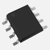
Part Details for NCP1230D100R2 by onsemi
Results Overview of NCP1230D100R2 by onsemi
- Distributor Offerings: (2 listings)
- Number of FFF Equivalents: (0 replacements)
- CAD Models: (Request Part)
- Number of Functional Equivalents: (2 options)
- Part Data Attributes: (Available)
- Reference Designs: (Not Available)
Tip: Data for a part may vary between manufacturers. You can filter for manufacturers on the top of the page next to the part image and part number.
NCP1230D100R2 Information
NCP1230D100R2 by onsemi is a Switching Regulator or Controller.
Switching Regulator or Controllers are under the broader part category of Power Circuits.
A power circuit delivers electricity in order to operate a load for an electronic device. Power circuits include transformers, generators and switches. Read more about Power Circuits on our Power Circuits part category page.
Price & Stock for NCP1230D100R2
| Part # | Distributor | Description | Stock | Price | Buy | |
|---|---|---|---|---|---|---|
|
DISTI #
86132936
|
Verical | Switching Mode Power Supply Controller Min Qty: 455 Package Multiple: 1 Date Code: 0401 | Americas - 2500 |
|
$0.6853 / $0.8256 | Buy Now |
|
|
Rochester Electronics | Switching Controller, Current-mode, 0.5A, 110kHz Switching Freq-Max, PDSO8 RoHS: Not Compliant Status: Obsolete Min Qty: 1 | 2500 |
|
$0.4095 / $0.6605 | Buy Now |
Part Details for NCP1230D100R2
NCP1230D100R2 CAD Models
NCP1230D100R2 Part Data Attributes
|
|
NCP1230D100R2
onsemi
Buy Now
Datasheet
|
Compare Parts:
NCP1230D100R2
onsemi
IC 0.5 A SWITCHING CONTROLLER, 110 kHz SWITCHING FREQ-MAX, PDSO8, SOIC-8, Switching Regulator or Controller
|
| Rohs Code | No | |
| Part Life Cycle Code | Obsolete | |
| Ihs Manufacturer | ONSEMI | |
| Part Package Code | SOIC | |
| Package Description | SOIC-8 | |
| Pin Count | 8 | |
| Reach Compliance Code | not_compliant | |
| ECCN Code | EAR99 | |
| HTS Code | 8542.39.00.01 | |
| Factory Lead Time | 4 Weeks | |
| Additional Feature | PULSE FREQUENCY MODULATION TECHNIQUE IS ALSO POSSIBLE | |
| Analog IC - Other Type | SWITCHING CONTROLLER | |
| Control Mode | CURRENT-MODE | |
| Control Technique | PULSE WIDTH MODULATION | |
| Input Voltage-Min | 8.4 V | |
| Input Voltage-Nom | 13 V | |
| JESD-30 Code | R-PDSO-G8 | |
| JESD-609 Code | e0 | |
| Length | 4.9 mm | |
| Moisture Sensitivity Level | 1 | |
| Number of Functions | 1 | |
| Number of Terminals | 8 | |
| Operating Temperature-Max | 125 °C | |
| Operating Temperature-Min | -40 °C | |
| Output Current-Max | 0.5 A | |
| Package Body Material | PLASTIC/EPOXY | |
| Package Code | SOP | |
| Package Equivalence Code | SOP8,.25 | |
| Package Shape | RECTANGULAR | |
| Package Style | SMALL OUTLINE | |
| Peak Reflow Temperature (Cel) | 235 | |
| Qualification Status | Not Qualified | |
| Seated Height-Max | 1.75 mm | |
| Surface Mount | YES | |
| Switcher Configuration | SINGLE | |
| Switching Frequency-Max | 110 kHz | |
| Temperature Grade | AUTOMOTIVE | |
| Terminal Finish | TIN LEAD | |
| Terminal Form | GULL WING | |
| Terminal Pitch | 1.27 mm | |
| Terminal Position | DUAL | |
| Width | 3.9 mm |
Alternate Parts for NCP1230D100R2
This table gives cross-reference parts and alternative options found for NCP1230D100R2. The Form Fit Function (FFF) tab will give you the options that are more likely to serve as direct pin-to-pin alternates or drop-in parts. The Functional Equivalents tab will give you options that are likely to match the same function of NCP1230D100R2, but it may not fit your design. Always verify details of parts you are evaluating, as these parts are offered as suggestions for what you are looking for and are not guaranteed.
| Part Number | Manufacturer | Composite Price | Description | Compare |
|---|---|---|---|---|
| NCP1230D100R2 | Rochester Electronics LLC | Check for Price | 0.5A SWITCHING CONTROLLER, 110kHz SWITCHING FREQ-MAX, PDSO8, SOIC-8 | NCP1230D100R2 vs NCP1230D100R2 |
| NCP1230D100R2G | onsemi | Check for Price | PWM Controller, Fixed Frequency, Current Mode, SOIC-8 Narrow Body, 2500-REEL | NCP1230D100R2 vs NCP1230D100R2G |
NCP1230D100R2 Frequently Asked Questions (FAQ)
-
The recommended PCB layout for optimal thermal performance involves placing the device on a thermal pad connected to a large copper area on the PCB, and ensuring good airflow around the device. A minimum of 2oz copper thickness is recommended.
-
To ensure reliable start-up, ensure that the input voltage rises monotonically and does not droop during start-up. Also, ensure that the output capacitor is properly sized to handle the inrush current during start-up.
-
The maximum allowed voltage on the EN pin is 6V. Exceeding this voltage may damage the device.
-
While it is possible to use a different inductor value, it is not recommended as it may affect the converter's performance and stability. The recommended inductor value is chosen to ensure optimal performance and efficiency.
-
To troubleshoot issues with the converter's output voltage, check the input voltage, output capacitor value, and inductor value. Also, ensure that the device is properly soldered and that there are no shorts or opens on the PCB.
