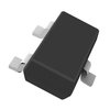
Part Details for MUN5231T1 by onsemi
Results Overview of MUN5231T1 by onsemi
- Distributor Offerings: (1 listing)
- Number of FFF Equivalents: (0 replacements)
- CAD Models: (Request Part)
- Number of Functional Equivalents: (0 options)
- Part Data Attributes: (Available)
- Reference Designs: (Not Available)
Tip: Data for a part may vary between manufacturers. You can filter for manufacturers on the top of the page next to the part image and part number.
MUN5231T1 Information
MUN5231T1 by onsemi is a Small Signal Bipolar Transistor.
Small Signal Bipolar Transistors are under the broader part category of Transistors.
A transistor is a small semiconductor device used to amplify, control, or create electrical signals. When selecting a transistor, factors such as voltage, current rating, gain, and power dissipation must be considered, with common types. Read more about Transistors on our Transistors part category page.
Price & Stock for MUN5231T1
| Part # | Distributor | Description | Stock | Price | Buy | |
|---|---|---|---|---|---|---|
|
|
Rochester Electronics | Small Signal Bipolar Transistor, 0.1A, 50V, NPN RoHS: Not Compliant Status: Obsolete Min Qty: 1 | 4250 |
|
$0.0410 / $0.0661 | Buy Now |
Part Details for MUN5231T1
MUN5231T1 CAD Models
MUN5231T1 Part Data Attributes
|
|
MUN5231T1
onsemi
Buy Now
Datasheet
|
Compare Parts:
MUN5231T1
onsemi
100mA, 50V, NPN, Si, SMALL SIGNAL TRANSISTOR, CASE 419-04, SC-70, 3 PIN
|
| Rohs Code | No | |
| Part Life Cycle Code | Obsolete | |
| Ihs Manufacturer | ONSEMI | |
| Part Package Code | SC-70 | |
| Package Description | CASE 419-04, SC-70, 3 PIN | |
| Pin Count | 3 | |
| Manufacturer Package Code | CASE 419-04 | |
| Reach Compliance Code | not_compliant | |
| ECCN Code | EAR99 | |
| Factory Lead Time | 4 Weeks | |
| Additional Feature | BUILT IN BIAS RESISTOR RATIO 1 | |
| Collector Current-Max (IC) | 0.1 A | |
| Collector-Emitter Voltage-Max | 50 V | |
| Configuration | SINGLE WITH BUILT-IN RESISTOR | |
| DC Current Gain-Min (hFE) | 8 | |
| JESD-30 Code | R-PDSO-G3 | |
| JESD-609 Code | e0 | |
| Moisture Sensitivity Level | 1 | |
| Number of Elements | 1 | |
| Number of Terminals | 3 | |
| Package Body Material | PLASTIC/EPOXY | |
| Package Shape | RECTANGULAR | |
| Package Style | SMALL OUTLINE | |
| Peak Reflow Temperature (Cel) | 235 | |
| Polarity/Channel Type | NPN | |
| Power Dissipation-Max (Abs) | 0.15 W | |
| Qualification Status | Not Qualified | |
| Surface Mount | YES | |
| Terminal Finish | Tin/Lead (Sn/Pb) | |
| Terminal Form | GULL WING | |
| Terminal Position | DUAL | |
| Time@Peak Reflow Temperature-Max (s) | 30 | |
| Transistor Application | SWITCHING | |
| Transistor Element Material | SILICON |
MUN5231T1 Frequently Asked Questions (FAQ)
-
A good PCB layout for the MUN5231T1 should prioritize thermal dissipation. Place the device near a thermal pad or a heat sink, and ensure good copper coverage around the device. Use thermal vias to connect the top and bottom layers, and avoid routing high-current traces near the device.
-
To ensure reliable operation at high temperatures, follow the recommended operating conditions, and consider derating the device's power dissipation. Implement a thermal management system, such as a heat sink or fan, to keep the junction temperature below the maximum rating. Monitor the device's temperature and adjust the system design accordingly.
-
The MUN5231T1's high voltage rating requires careful PCB design to prevent electrical overstress. Ensure a sufficient creepage distance between high-voltage traces and other conductive elements. Use a suitable PCB material with high dielectric strength, and consider adding guard rings or electrostatic discharge (ESD) protection devices.
-
Choose an input capacitor with a high voltage rating, low equivalent series resistance (ESR), and a suitable capacitance value. The capacitor should be able to handle the maximum input voltage and ripple current. Consider using a ceramic or film capacitor with a voltage rating at least 1.5 times the maximum input voltage.
-
To minimize EMI and ensure EMC, follow good design practices such as using a shielded enclosure, keeping high-frequency traces short, and using EMI filters or common-mode chokes. Ensure the system meets the relevant regulatory standards, such as CISPR or FCC, and perform EMI testing to validate the design.
