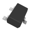
Part Details for MSD42WT1 by onsemi
Results Overview of MSD42WT1 by onsemi
- Distributor Offerings: (2 listings)
- Number of FFF Equivalents: (0 replacements)
- CAD Models: (Request Part)
- Number of Functional Equivalents: (0 options)
- Part Data Attributes: (Available)
- Reference Designs: (Not Available)
Tip: Data for a part may vary between manufacturers. You can filter for manufacturers on the top of the page next to the part image and part number.
MSD42WT1 Information
MSD42WT1 by onsemi is a Small Signal Bipolar Transistor.
Small Signal Bipolar Transistors are under the broader part category of Transistors.
A transistor is a small semiconductor device used to amplify, control, or create electrical signals. When selecting a transistor, factors such as voltage, current rating, gain, and power dissipation must be considered, with common types. Read more about Transistors on our Transistors part category page.
Price & Stock for MSD42WT1
| Part # | Distributor | Description | Stock | Price | Buy | |
|---|---|---|---|---|---|---|
|
DISTI #
86122154
|
Verical | Trans GP BJT NPN 300V 0.15A 150mW 3-Pin SC-70 T/R Min Qty: 6834 Package Multiple: 1 Date Code: 0401 | Americas - 14320 |
|
$0.0410 / $0.0549 | Buy Now |
|
|
Rochester Electronics | Small Signal Bipolar Transistor, 0.15A, 300V, NPN RoHS: Not Compliant Status: Obsolete Min Qty: 1 | 14320 |
|
$0.0328 / $0.0529 | Buy Now |
Part Details for MSD42WT1
MSD42WT1 CAD Models
MSD42WT1 Part Data Attributes
|
|
MSD42WT1
onsemi
Buy Now
Datasheet
|
Compare Parts:
MSD42WT1
onsemi
TRANSISTOR 150 mA, 300 V, NPN, Si, SMALL SIGNAL TRANSISTOR, CASE 419-04, SC-70, 3 PIN, BIP General Purpose Small Signal
|
| Rohs Code | No | |
| Part Life Cycle Code | Obsolete | |
| Ihs Manufacturer | ONSEMI | |
| Part Package Code | SC-70 | |
| Package Description | CASE 419-04, SC-70, 3 PIN | |
| Pin Count | 3 | |
| Manufacturer Package Code | CASE 419-04 | |
| Reach Compliance Code | not_compliant | |
| ECCN Code | EAR99 | |
| Factory Lead Time | 4 Weeks | |
| Collector Current-Max (IC) | 0.15 A | |
| Collector-Emitter Voltage-Max | 300 V | |
| Configuration | SINGLE | |
| DC Current Gain-Min (hFE) | 40 | |
| JESD-30 Code | R-PDSO-G3 | |
| JESD-609 Code | e0 | |
| Moisture Sensitivity Level | 1 | |
| Number of Elements | 1 | |
| Number of Terminals | 3 | |
| Operating Temperature-Max | 150 °C | |
| Package Body Material | PLASTIC/EPOXY | |
| Package Shape | RECTANGULAR | |
| Package Style | SMALL OUTLINE | |
| Peak Reflow Temperature (Cel) | 235 | |
| Polarity/Channel Type | NPN | |
| Power Dissipation-Max (Abs) | 0.15 W | |
| Qualification Status | Not Qualified | |
| Surface Mount | YES | |
| Terminal Finish | TIN LEAD | |
| Terminal Form | GULL WING | |
| Terminal Position | DUAL | |
| Transistor Application | AMPLIFIER | |
| Transistor Element Material | SILICON |
MSD42WT1 Frequently Asked Questions (FAQ)
-
A good PCB layout for the MSD42WT1 should include a solid copper pour on the top and bottom layers, connected to the thermal pad through multiple vias. This helps to dissipate heat efficiently. Additionally, keep the thermal pad away from other components and ensure good airflow around the device.
-
The input capacitor value depends on the input voltage, output voltage, and switching frequency. A general rule of thumb is to choose a capacitor with a value between 10uF to 22uF, with a voltage rating at least 1.5 times the input voltage. Consult the application note or onsemi's capacitor selection guide for more specific guidance.
-
The maximum allowed voltage drop across the internal FETs is not explicitly stated in the datasheet. However, as a general guideline, it's recommended to keep the voltage drop below 1V to ensure reliable operation and minimize power losses.
-
The MSD42WT1 is rated for operation up to 150°C, but it's essential to consider the derating curves and thermal management when operating in high-temperature environments. Ensure proper heat sinking, and consider using a heat sink or thermal interface material to maintain a safe junction temperature.
-
Start by verifying the input voltage, output voltage, and switching frequency. Check for proper PCB layout, component selection, and soldering quality. Use an oscilloscope to monitor the output voltage and switching node waveforms. Consult the application note, datasheet, and onsemi's support resources for further guidance.
