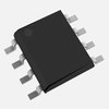
Part Details for MC9S08QA2CDNE by Freescale Semiconductor
Results Overview of MC9S08QA2CDNE by Freescale Semiconductor
- Distributor Offerings: (1 listing)
- Number of FFF Equivalents: (1 replacement)
- CAD Models: (Request Part)
- Number of Functional Equivalents: (10 options)
- Part Data Attributes: (Available)
- Reference Designs: (Not Available)
Tip: Data for a part may vary between manufacturers. You can filter for manufacturers on the top of the page next to the part image and part number.
MC9S08QA2CDNE Information
MC9S08QA2CDNE by Freescale Semiconductor is a Microcontroller.
Microcontrollers are under the broader part category of Microcontrollers and Processors.
Microcontrollers (MCUs) are small, low-power integrated circuits used to control embedded systems. Microcontrollers are primarily used to automate and control devices. Read more about Microcontrollers and Processors on our Microcontrollers and Processors part category page.
Price & Stock for MC9S08QA2CDNE
| Part # | Distributor | Description | Stock | Price | Buy | |
|---|---|---|---|---|---|---|
|
|
Rochester Electronics | MC9S08QA2CDNE - S08QA 8-bit MCU, S08 core, 2KB Flash, 20MHz, SOIC 8 RoHS: Compliant Status: Active Min Qty: 1 | 30 |
|
$1.3800 / $1.7200 | Buy Now |
Part Details for MC9S08QA2CDNE
MC9S08QA2CDNE CAD Models
MC9S08QA2CDNE Part Data Attributes
|
|
MC9S08QA2CDNE
Freescale Semiconductor
Buy Now
Datasheet
|
Compare Parts:
MC9S08QA2CDNE
Freescale Semiconductor
8-BIT, FLASH, 20MHz, MICROCONTROLLER, PDSO8, ROHS COMPLIANT, MS-012AA, SOIC-8
|
| Pbfree Code | Yes | |
| Rohs Code | Yes | |
| Part Life Cycle Code | Transferred | |
| Ihs Manufacturer | FREESCALE SEMICONDUCTOR INC | |
| Part Package Code | SOIC | |
| Package Description | ROHS COMPLIANT, MS-012AA, SOIC-8 | |
| Pin Count | 8 | |
| Reach Compliance Code | compliant | |
| ECCN Code | 3A991.A.2 | |
| HTS Code | 8542.31.00.01 | |
| Has ADC | YES | |
| Address Bus Width | ||
| Bit Size | 8 | |
| Clock Frequency-Max | 20 MHz | |
| DAC Channels | NO | |
| DMA Channels | NO | |
| External Data Bus Width | ||
| JESD-30 Code | R-PDSO-G8 | |
| JESD-609 Code | e3 | |
| Length | 4.9 mm | |
| Moisture Sensitivity Level | 3 | |
| Number of I/O Lines | 6 | |
| Number of Terminals | 8 | |
| On Chip Program ROM Width | 8 | |
| Operating Temperature-Max | 85 °C | |
| Operating Temperature-Min | -40 °C | |
| PWM Channels | YES | |
| Package Body Material | PLASTIC/EPOXY | |
| Package Code | SOP | |
| Package Equivalence Code | SOP8,.25 | |
| Package Shape | RECTANGULAR | |
| Package Style | SMALL OUTLINE | |
| Peak Reflow Temperature (Cel) | 260 | |
| Qualification Status | Not Qualified | |
| RAM (bytes) | 160 | |
| ROM (words) | 2048 | |
| ROM Programmability | FLASH | |
| Seated Height-Max | 1.75 mm | |
| Speed | 20 MHz | |
| Supply Current-Max | 5 mA | |
| Supply Voltage-Max | 3.6 V | |
| Supply Voltage-Min | 1.8 V | |
| Supply Voltage-Nom | 3 V | |
| Surface Mount | YES | |
| Technology | CMOS | |
| Temperature Grade | INDUSTRIAL | |
| Terminal Finish | MATTE TIN | |
| Terminal Form | GULL WING | |
| Terminal Pitch | 1.27 mm | |
| Terminal Position | DUAL | |
| Time@Peak Reflow Temperature-Max (s) | 40 | |
| Width | 3.9 mm | |
| uPs/uCs/Peripheral ICs Type | MICROCONTROLLER |
Alternate Parts for MC9S08QA2CDNE
This table gives cross-reference parts and alternative options found for MC9S08QA2CDNE. The Form Fit Function (FFF) tab will give you the options that are more likely to serve as direct pin-to-pin alternates or drop-in parts. The Functional Equivalents tab will give you options that are likely to match the same function of MC9S08QA2CDNE, but it may not fit your design. Always verify details of parts you are evaluating, as these parts are offered as suggestions for what you are looking for and are not guaranteed.
| Part Number | Manufacturer | Composite Price | Description | Compare |
|---|---|---|---|---|
| MC9S08QA2CDNE | Rochester Electronics LLC | Check for Price | 8-BIT, FLASH, 20 MHz, MICROCONTROLLER, PDSO8, ROHS COMPLIANT, MS-012AA, SOIC-8 | MC9S08QA2CDNE vs MC9S08QA2CDNE |
MC9S08QA2CDNE Frequently Asked Questions (FAQ)
-
The maximum operating frequency of the MC9S08QA2CDNE is 20 MHz, but it can be overclocked to 25 MHz with some limitations.
-
The internal clock source can be configured using the SYNR and REFS registers. The SYNR register sets the clock source, and the REFS register sets the clock frequency.
-
The VLLS mode is a low-power mode that reduces power consumption to a minimum. It is used to save power when the device is not in use, and can be used in conjunction with other low-power modes.
-
The ADC module can be used to convert analog signals to digital values. The ADC can be configured using the ADCSC1 and ADCSC2 registers, and the conversion result can be read from the ADCRH and ADCRL registers.
-
The maximum current that can be sourced or sunk by the GPIO pins is 25 mA, but this can be limited by the device's power supply and the external circuitry.
