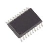
Part Details for MC75174BDWR2G by onsemi
Results Overview of MC75174BDWR2G by onsemi
- Distributor Offerings: (1 listing)
- Number of FFF Equivalents: (1 replacement)
- CAD Models: (Request Part)
- Number of Functional Equivalents: (10 options)
- Part Data Attributes: (Available)
- Reference Designs: (Not Available)
Tip: Data for a part may vary between manufacturers. You can filter for manufacturers on the top of the page next to the part image and part number.
MC75174BDWR2G Information
MC75174BDWR2G by onsemi is a Line Driver or Receiver.
Line Driver or Receivers are under the broader part category of Drivers And Interfaces.
A driver controls the current or voltage delivered to components like LCDs or motors, while an interface component connects systems for data transfer and control. Read more about Drivers And Interfaces on our Drivers And Interfaces part category page.
Price & Stock for MC75174BDWR2G
| Part # | Distributor | Description | Stock | Price | Buy | |
|---|---|---|---|---|---|---|
|
DISTI #
MC75174BDWR2G
|
Avnet Americas | - Tape and Reel (Alt: MC75174BDWR2G) RoHS: Compliant Min Qty: 1000 Package Multiple: 1000 Lead time: 111 Weeks, 0 Days Container: Reel | 0 |
|
RFQ |
Part Details for MC75174BDWR2G
MC75174BDWR2G CAD Models
MC75174BDWR2G Part Data Attributes
|
|
MC75174BDWR2G
onsemi
Buy Now
Datasheet
|
Compare Parts:
MC75174BDWR2G
onsemi
Quad Line Driver with Three-State Output (EIA-485 ), SOIC-20 WB, 1000-REEL
|
| Pbfree Code | Yes | |
| Part Life Cycle Code | Obsolete | |
| Ihs Manufacturer | ON SEMICONDUCTOR | |
| Part Package Code | SOIC-20 WB | |
| Package Description | SOP, SOP20,.4 | |
| Pin Count | 20 | |
| Manufacturer Package Code | 751D-05 | |
| Reach Compliance Code | unknown | |
| ECCN Code | EAR99 | |
| HTS Code | 8542.39.00.01 | |
| Factory Lead Time | 111 Weeks | |
| Samacsys Manufacturer | onsemi | |
| Differential Output | YES | |
| Driver Number of Bits | 4 | |
| High Level Input Current-Max | 0.00002 A | |
| Input Characteristics | STANDARD | |
| Interface IC Type | LINE DRIVER | |
| Interface Standard | V.11; X.27; EIA-422-A; EIA-485 | |
| JESD-30 Code | R-PDSO-G20 | |
| JESD-609 Code | e3 | |
| Length | 12.8 mm | |
| Moisture Sensitivity Level | 3 | |
| Number of Functions | 4 | |
| Number of Terminals | 20 | |
| Operating Temperature-Max | 85 °C | |
| Operating Temperature-Min | -40 °C | |
| Out Swing-Min | 1.5 V | |
| Output Characteristics | 3-STATE | |
| Package Body Material | PLASTIC/EPOXY | |
| Package Code | SOP | |
| Package Equivalence Code | SOP20,.4 | |
| Package Shape | RECTANGULAR | |
| Package Style | SMALL OUTLINE | |
| Peak Reflow Temperature (Cel) | 260 | |
| Qualification Status | Not Qualified | |
| Seated Height-Max | 2.65 mm | |
| Supply Voltage-Max | 5.25 V | |
| Supply Voltage-Min | 4.75 V | |
| Supply Voltage-Nom | 5 V | |
| Surface Mount | YES | |
| Technology | BIPOLAR | |
| Temperature Grade | INDUSTRIAL | |
| Terminal Finish | Tin (Sn) | |
| Terminal Form | GULL WING | |
| Terminal Pitch | 1.27 mm | |
| Terminal Position | DUAL | |
| Time@Peak Reflow Temperature-Max (s) | 40 | |
| Transmit Delay-Max | 25 ns | |
| Width | 7.5 mm |
Alternate Parts for MC75174BDWR2G
This table gives cross-reference parts and alternative options found for MC75174BDWR2G. The Form Fit Function (FFF) tab will give you the options that are more likely to serve as direct pin-to-pin alternates or drop-in parts. The Functional Equivalents tab will give you options that are likely to match the same function of MC75174BDWR2G, but it may not fit your design. Always verify details of parts you are evaluating, as these parts are offered as suggestions for what you are looking for and are not guaranteed.
| Part Number | Manufacturer | Composite Price | Description | Compare |
|---|---|---|---|---|
| MC75174BDW | onsemi | Check for Price | Quad Line Driver with Three-State Output (EIA-485 ), SOIC-20 WB, 75-TUBE | MC75174BDWR2G vs MC75174BDW |
MC75174BDWR2G Frequently Asked Questions (FAQ)
-
A good thermal design is crucial for the MC75174BDWR2G. It's recommended to use a 2-layer or 4-layer PCB with a solid ground plane, and to place thermal vias under the device to dissipate heat efficiently. A minimum of 2 oz copper thickness is recommended for the top and bottom layers.
-
To ensure reliable operation in high-temperature environments, it's essential to follow the recommended operating conditions and derating guidelines. Make sure to provide adequate heat sinking, and consider using a thermal interface material (TIM) to improve heat transfer between the device and the heat sink.
-
The recommended input capacitor is a 10 μF ceramic capacitor with X7R or X5R dielectric, and the recommended output capacitor is a 22 μF ceramic capacitor with X7R or X5R dielectric. These capacitors should be placed as close to the device as possible to minimize parasitic inductance.
-
To troubleshoot issues with the output voltage regulation, check the input voltage, output load, and feedback resistors. Ensure that the input voltage is within the recommended range, the output load is within the specified current limit, and the feedback resistors are correctly configured. Also, verify that the device is properly soldered and that there are no signs of overheating.
-
Yes, the MC75174BDWR2G can be used in a switching regulator application. However, it's essential to follow the recommended switching frequency, duty cycle, and output filter design to ensure stable operation and minimize electromagnetic interference (EMI).
