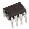
Part Details for MC34262P by onsemi
Results Overview of MC34262P by onsemi
- Distributor Offerings: (4 listings)
- Number of FFF Equivalents: (0 replacements)
- CAD Models: (Request Part)
- Number of Functional Equivalents: (0 options)
- Part Data Attributes: (Available)
- Reference Designs: (Not Available)
Tip: Data for a part may vary between manufacturers. You can filter for manufacturers on the top of the page next to the part image and part number.
MC34262P Information
MC34262P by onsemi is a Switching Regulator or Controller.
Switching Regulator or Controllers are under the broader part category of Power Circuits.
A power circuit delivers electricity in order to operate a load for an electronic device. Power circuits include transformers, generators and switches. Read more about Power Circuits on our Power Circuits part category page.
Price & Stock for MC34262P
| Part # | Distributor | Description | Stock | Price | Buy | |
|---|---|---|---|---|---|---|
|
|
Bristol Electronics | Min Qty: 3 | 76 |
|
$1.0969 / $1.7550 | Buy Now |
|
|
Quest Components | 0.5A POWER FACTOR CONTROLLER, PDIP8 | 60 |
|
$0.8775 / $2.3400 | Buy Now |
|
|
Component Electronics, Inc | IN STOCK SHIP TODAY | 48 |
|
$1.2500 / $1.9200 | Buy Now |
|
|
Cytech Systems Limited | IC PFC CTRLR CRM 8DIP | 2500 |
|
RFQ |
Part Details for MC34262P
MC34262P CAD Models
MC34262P Part Data Attributes
|
|
MC34262P
onsemi
Buy Now
Datasheet
|
Compare Parts:
MC34262P
onsemi
0.5A POWER FACTOR CONTROLLER, PDIP8, PLASTIC, DIP-8
|
| Rohs Code | No | |
| Part Life Cycle Code | Obsolete | |
| Ihs Manufacturer | ONSEMI | |
| Part Package Code | DIP | |
| Package Description | PLASTIC, DIP-8 | |
| Pin Count | 8 | |
| Reach Compliance Code | not_compliant | |
| ECCN Code | EAR99 | |
| HTS Code | 8542.39.00.01 | |
| Samacsys Manufacturer | onsemi | |
| Analog IC - Other Type | POWER FACTOR CONTROLLER | |
| Control Mode | CURRENT-MODE | |
| Control Technique | PULSE WIDTH MODULATION | |
| Input Voltage-Max | 30 V | |
| Input Voltage-Min | 9 V | |
| Input Voltage-Nom | 12 V | |
| JESD-30 Code | R-PDIP-T8 | |
| JESD-609 Code | e0 | |
| Length | 9.78 mm | |
| Number of Functions | 1 | |
| Number of Terminals | 8 | |
| Operating Temperature-Max | 85 °C | |
| Operating Temperature-Min | ||
| Output Current-Max | 0.5 A | |
| Package Body Material | PLASTIC/EPOXY | |
| Package Code | DIP | |
| Package Equivalence Code | DIP8,.3 | |
| Package Shape | RECTANGULAR | |
| Package Style | IN-LINE | |
| Peak Reflow Temperature (Cel) | 235 | |
| Qualification Status | Not Qualified | |
| Seated Height-Max | 4.45 mm | |
| Surface Mount | NO | |
| Switcher Configuration | SINGLE | |
| Technology | BIPOLAR | |
| Temperature Grade | OTHER | |
| Terminal Finish | TIN LEAD | |
| Terminal Form | THROUGH-HOLE | |
| Terminal Pitch | 2.54 mm | |
| Terminal Position | DUAL | |
| Width | 7.62 mm |
MC34262P Frequently Asked Questions (FAQ)
-
A good thermal design is crucial for the MC34262P. It's recommended to have a solid copper plane under the IC, and to use thermal vias to connect the plane to the top layer. Additionally, keep the thermal pad clear of any obstacles and ensure good airflow around the device.
-
To ensure reliable operation in high-temperature environments, it's essential to follow proper thermal design guidelines, use a suitable heat sink, and ensure good airflow. Also, consider derating the device's power dissipation according to the temperature derating curve provided in the datasheet.
-
The recommended input capacitor is a 10uF ceramic capacitor with a voltage rating of at least 25V. For the output capacitor, a 22uF ceramic capacitor with a voltage rating of at least 25V is recommended. These values can be adjusted based on the specific application requirements.
-
To troubleshoot issues with the enable pin (EN), ensure that the pin is properly connected to a logic-level signal (either 0V or VCC). Also, verify that the pin is not floating or connected to an incorrect voltage level. If issues persist, check the device's datasheet for specific enable pin requirements.
-
When powering up a system with multiple MC34262P devices, it's recommended to sequence the power supplies to prevent unwanted current surges. Power up the input voltage (VIN) first, followed by the enable pin (EN), and then the output voltage (VOUT). This ensures that the devices are properly enabled and configured before the output voltage is applied.
