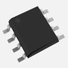
Part Details for MC33340DR2G by onsemi
Results Overview of MC33340DR2G by onsemi
- Distributor Offerings: (1 listing)
- Number of FFF Equivalents: (0 replacements)
- CAD Models: (Request Part)
- Number of Functional Equivalents: (5 options)
- Part Data Attributes: (Available)
- Reference Designs: (Not Available)
Tip: Data for a part may vary between manufacturers. You can filter for manufacturers on the top of the page next to the part image and part number.
MC33340DR2G Information
MC33340DR2G by onsemi is a Power Management Circuit.
Power Management Circuits are under the broader part category of Power Circuits.
A power circuit delivers electricity in order to operate a load for an electronic device. Power circuits include transformers, generators and switches. Read more about Power Circuits on our Power Circuits part category page.
Price & Stock for MC33340DR2G
| Part # | Distributor | Description | Stock | Price | Buy | |
|---|---|---|---|---|---|---|
|
|
Win Source Electronics | IC CTRLR BATT FAST CHARGE 8-SOIC | 8110 |
|
$2.1667 / $3.2501 | Buy Now |
Part Details for MC33340DR2G
MC33340DR2G CAD Models
MC33340DR2G Part Data Attributes
|
|
MC33340DR2G
onsemi
Buy Now
Datasheet
|
Compare Parts:
MC33340DR2G
onsemi
NiCd/NiMH Battery Fast Charge Controller, SOIC-8 Narrow Body, 2500-REEL
|
| Pbfree Code | Yes | |
| Rohs Code | Yes | |
| Part Life Cycle Code | Obsolete | |
| Ihs Manufacturer | ONSEMI | |
| Part Package Code | SOIC-8 Narrow Body | |
| Pin Count | 8 | |
| Manufacturer Package Code | 751-07 | |
| Reach Compliance Code | unknown | |
| ECCN Code | EAR99 | |
| HTS Code | 8542.39.00.01 | |
| Samacsys Manufacturer | onsemi | |
| Analog IC - Other Type | POWER SUPPLY SUPPORT CIRCUIT | |
| Control Mode | VOLTAGE-MODE | |
| Control Technique | PULSE WIDTH MODULATION | |
| Input Voltage-Max | 18 V | |
| Input Voltage-Min | 3 V | |
| Input Voltage-Nom | 6 V | |
| JESD-609 Code | e3 | |
| Output Current-Max | 0.05 A | |
| Peak Reflow Temperature (Cel) | 260 | |
| Qualification Status | Not Qualified | |
| Switcher Configuration | SINGLE | |
| Switching Frequency-Max | 760 kHz | |
| Temperature Grade | OTHER | |
| Terminal Finish | TIN |
Alternate Parts for MC33340DR2G
This table gives cross-reference parts and alternative options found for MC33340DR2G. The Form Fit Function (FFF) tab will give you the options that are more likely to serve as direct pin-to-pin alternates or drop-in parts. The Functional Equivalents tab will give you options that are likely to match the same function of MC33340DR2G, but it may not fit your design. Always verify details of parts you are evaluating, as these parts are offered as suggestions for what you are looking for and are not guaranteed.
| Part Number | Manufacturer | Composite Price | Description | Compare |
|---|---|---|---|---|
| MC33340DR2 | onsemi | Check for Price | NiCd/NiMH Battery Fast Charge Controller, SOIC-8 Narrow Body, 2500-REEL | MC33340DR2G vs MC33340DR2 |
| MC33340D | onsemi | Check for Price | NiCd/NiMH Battery Fast Charge Controller, SOIC-8 Narrow Body, 98-TUBE | MC33340DR2G vs MC33340D |
| MC33340DR2 | Rochester Electronics LLC | Check for Price | 0.05A BATTERY CHARGE CONTROLLER, 760kHz SWITCHING FREQ-MAX, PDSO8, SOIC-8 | MC33340DR2G vs MC33340DR2 |
| MC33340DR2 | Motorola Mobility LLC | Check for Price | BATTERY CHARGE CONTROLLER, 760kHz SWITCHING FREQ-MAX, PDSO8, PLASTIC, SO-8 | MC33340DR2G vs MC33340DR2 |
| MC33340DG | onsemi | Check for Price | NiCd/NiMH Battery Fast Charge Controller, SOIC-8 Narrow Body, 98-TUBE | MC33340DR2G vs MC33340DG |
MC33340DR2G Frequently Asked Questions (FAQ)
-
A good PCB layout is crucial for the MC33340DR2G. Ensure a solid ground plane, keep the input and output traces separate, and use a common mode choke to reduce EMI. Refer to the onsemi application note AND8327/D for a recommended layout.
-
The input capacitor value depends on the input voltage, output voltage, and desired ripple voltage. A general rule of thumb is to use a capacitor with a value between 1uF to 10uF. Consult the datasheet and onsemi's capacitor selection guide for more information.
-
The MC33340DR2G is rated for operation up to 125°C ambient temperature. However, it's recommended to derate the device for reliable operation above 85°C. Consult the datasheet for thermal derating information.
-
To ensure proper power-up and power-down, follow the recommended power sequencing in the datasheet. Apply the input voltage before enabling the device, and disable the device before removing the input voltage.
-
To minimize EMI, use a common mode choke, add a ferrite bead to the input, and ensure a good PCB layout. Additionally, consider adding a shield or a metal can to the device. Consult the datasheet and onsemi's EMI reduction guide for more information.
