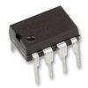
Part Details for M24C16-BN6 by STMicroelectronics
Results Overview of M24C16-BN6 by STMicroelectronics
- Distributor Offerings: (1 listing)
- Number of FFF Equivalents: (0 replacements)
- CAD Models: (Request Part)
- Number of Functional Equivalents: (0 options)
- Part Data Attributes: (Available)
- Reference Designs: (Not Available)
Tip: Data for a part may vary between manufacturers. You can filter for manufacturers on the top of the page next to the part image and part number.
M24C16-BN6 Information
M24C16-BN6 by STMicroelectronics is an EEPROM.
EEPROMs are under the broader part category of Memory Components.
Memory components are essential in electronics for computer processing. They can be volatile or non-volatile, depending on the desired function. Read more about Memory Components on our Memory part category page.
Price & Stock for M24C16-BN6
| Part # | Distributor | Description | Stock | Price | Buy | |
|---|---|---|---|---|---|---|
|
|
Quest Components | EEPROM, 2KX8, SERIAL, CMOS, PDIP8 | 2 |
|
$2.0700 / $2.2500 | Buy Now |
Part Details for M24C16-BN6
M24C16-BN6 CAD Models
M24C16-BN6 Part Data Attributes
|
|
M24C16-BN6
STMicroelectronics
Buy Now
Datasheet
|
Compare Parts:
M24C16-BN6
STMicroelectronics
2KX8 I2C/2-WIRE SERIAL EEPROM, PDIP8, PLASTIC, DIP-8
|
| Pbfree Code | No | |
| Rohs Code | No | |
| Part Life Cycle Code | Obsolete | |
| Ihs Manufacturer | STMICROELECTRONICS | |
| Part Package Code | DIP | |
| Package Description | PLASTIC, DIP-8 | |
| Pin Count | 8 | |
| Reach Compliance Code | not_compliant | |
| ECCN Code | EAR99 | |
| HTS Code | 8542.32.00.51 | |
| Samacsys Manufacturer | STMicroelectronics | |
| Clock Frequency-Max (fCLK) | 0.4 MHz | |
| Data Retention Time-Min | 40 | |
| Endurance | 1000000 Write/Erase Cycles | |
| I2C Control Byte | 1010MMMR | |
| JESD-30 Code | R-PDIP-T8 | |
| JESD-609 Code | e0 | |
| Length | 9.27 mm | |
| Memory Density | 16384 bit | |
| Memory IC Type | EEPROM | |
| Memory Width | 8 | |
| Number of Functions | 1 | |
| Number of Terminals | 8 | |
| Number of Words | 2048 words | |
| Number of Words Code | 2000 | |
| Operating Mode | SYNCHRONOUS | |
| Operating Temperature-Max | 85 °C | |
| Operating Temperature-Min | -40 °C | |
| Organization | 2KX8 | |
| Output Characteristics | OPEN-DRAIN | |
| Package Body Material | PLASTIC/EPOXY | |
| Package Code | DIP | |
| Package Equivalence Code | DIP8,.3 | |
| Package Shape | RECTANGULAR | |
| Package Style | IN-LINE | |
| Parallel/Serial | SERIAL | |
| Qualification Status | Not Qualified | |
| Screening Level | AEC-Q100 | |
| Seated Height-Max | 5.33 mm | |
| Serial Bus Type | I2C | |
| Standby Current-Max | 0.000001 A | |
| Supply Current-Max | 0.002 mA | |
| Supply Voltage-Max (Vsup) | 5.5 V | |
| Supply Voltage-Min (Vsup) | 4.5 V | |
| Supply Voltage-Nom (Vsup) | 5 V | |
| Surface Mount | NO | |
| Technology | CMOS | |
| Temperature Grade | INDUSTRIAL | |
| Terminal Finish | TIN LEAD | |
| Terminal Form | THROUGH-HOLE | |
| Terminal Pitch | 2.54 mm | |
| Terminal Position | DUAL | |
| Width | 7.62 mm | |
| Write Cycle Time-Max (tWC) | 5 ms | |
| Write Protection | HARDWARE |
M24C16-BN6 Frequently Asked Questions (FAQ)
-
The maximum clock frequency for the M24C16-BN6 is 1 MHz, as specified in the datasheet. However, it's recommended to operate at a lower frequency, typically 400 kHz, to ensure reliable communication and minimize power consumption.
-
To handle multiple slave devices on the same I2C bus, ensure each device has a unique address. The M24C16-BN6 has three address pins (A0, A1, and A2) that can be connected to VCC or GND to set the device address. Use the address pins to assign a unique address to each device, and then use the I2C bus protocol to communicate with each device individually.
-
The M24C16-BN6 has a write endurance of 1 million cycles per page. A page is 16 bytes, and the device has 1024 pages. This means the device can withstand a total of 16,777,216 write cycles (1 million cycles/page * 1024 pages).
-
Implement a retry mechanism by detecting and handling I2C bus errors, such as ACK/NAK errors or bus timeouts. Use a software-based approach to retry the I2C transaction a specified number of times before considering the communication failed. This helps to improve the reliability of the I2C communication with the M24C16-BN6.
-
The M24C16-BN6 has a power-on reset (POR) circuit that initializes the device to its default state when the power supply is turned on. The POR circuit ensures that the device is in a known state after power-up, which helps to prevent unexpected behavior or data corruption.
