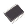
Part Details for LTC7545ACSW by Linear Technology
Results Overview of LTC7545ACSW by Linear Technology
- Distributor Offerings: (2 listings)
- Number of FFF Equivalents: (4 replacements)
- CAD Models: (Request Part)
- Number of Functional Equivalents: (10 options)
- Part Data Attributes: (Available)
- Reference Designs: (Not Available)
Tip: Data for a part may vary between manufacturers. You can filter for manufacturers on the top of the page next to the part image and part number.
LTC7545ACSW Information
LTC7545ACSW by Linear Technology is a Digital to Analog Converter.
Digital to Analog Converters are under the broader part category of Converters.
A converter is an electrical circuit that transforms electric energy into a different form that will support a elecrical load needed by a device. Read more about Converters on our Converters part category page.
Price & Stock for LTC7545ACSW
| Part # | Distributor | Description | Stock | Price | Buy | |
|---|---|---|---|---|---|---|
|
|
Bristol Electronics | 18 |
|
RFQ | ||
|
|
Quest Components | D/A CONVERTER, 1 FUNC, PARALLEL, WORD INPUT LOADING, PDSO20 | 14 |
|
$11.3600 / $12.7800 | Buy Now |
Part Details for LTC7545ACSW
LTC7545ACSW CAD Models
LTC7545ACSW Part Data Attributes
|
|
LTC7545ACSW
Linear Technology
Buy Now
Datasheet
|
Compare Parts:
LTC7545ACSW
Linear Technology
LTC7545A - Improved Industry Standard Parallel 12-Bit Multiplying DAC; Package: SO; Pins: 20; Temperature Range: 0°C to 70°C
|
| Rohs Code | No | |
| Part Life Cycle Code | Transferred | |
| Ihs Manufacturer | LINEAR TECHNOLOGY CORP | |
| Part Package Code | SOIC | |
| Package Description | 0.300 INCH, PLASTIC, SOP-20 | |
| Pin Count | 20 | |
| Manufacturer Package Code | SW | |
| Reach Compliance Code | not_compliant | |
| HTS Code | 8542.39.00.01 | |
| Analog Output Voltage-Max | 10 V | |
| Analog Output Voltage-Min | ||
| Converter Type | D/A CONVERTER | |
| Input Bit Code | BINARY, OFFSET BINARY | |
| Input Format | PARALLEL, WORD | |
| JESD-30 Code | R-PDSO-G20 | |
| JESD-609 Code | e0 | |
| Length | 12.8 mm | |
| Linearity Error-Max (EL) | 0.0122% | |
| Moisture Sensitivity Level | 1 | |
| Number of Bits | 12 | |
| Number of Functions | 1 | |
| Number of Terminals | 20 | |
| Operating Temperature-Max | 85 °C | |
| Operating Temperature-Min | -40 °C | |
| Package Body Material | PLASTIC/EPOXY | |
| Package Code | SOP | |
| Package Equivalence Code | SOP20,.4 | |
| Package Shape | RECTANGULAR | |
| Package Style | SMALL OUTLINE | |
| Qualification Status | Not Qualified | |
| Seated Height-Max | 2.65 mm | |
| Settling Time-Max | 1 µs | |
| Supply Current-Max | 2 mA | |
| Supply Voltage-Nom | 15 V | |
| Surface Mount | YES | |
| Technology | CMOS | |
| Temperature Grade | INDUSTRIAL | |
| Terminal Finish | TIN LEAD | |
| Terminal Form | GULL WING | |
| Terminal Pitch | 1.27 mm | |
| Terminal Position | DUAL | |
| Width | 7.5 mm |
Alternate Parts for LTC7545ACSW
This table gives cross-reference parts and alternative options found for LTC7545ACSW. The Form Fit Function (FFF) tab will give you the options that are more likely to serve as direct pin-to-pin alternates or drop-in parts. The Functional Equivalents tab will give you options that are likely to match the same function of LTC7545ACSW, but it may not fit your design. Always verify details of parts you are evaluating, as these parts are offered as suggestions for what you are looking for and are not guaranteed.
| Part Number | Manufacturer | Composite Price | Description | Compare |
|---|---|---|---|---|
| LTC7545AKSW#PBF | Analog Devices Inc | $7.6121 | Improved Industry Standard Parallel 12-Bit Multiplying DAC | LTC7545ACSW vs LTC7545AKSW#PBF |
| LTC7545ALSW#TR | Analog Devices Inc | Check for Price | D/A Converter, 1 Func, Parallel, Word Input Loading, PDSO20 | LTC7545ACSW vs LTC7545ALSW#TR |
| LTC7545ABSW#TRPBF | Analog Devices Inc | Check for Price | Improved Industry Standard Parallel 12-Bit Multiplying DAC | LTC7545ACSW vs LTC7545ABSW#TRPBF |
| LTC7545ALSW | Linear Technology | Check for Price | LTC7545A - Improved Industry Standard Parallel 12-Bit Multiplying DAC; Package: SO; Pins: 20; Temperature Range: 0°C to 70°C | LTC7545ACSW vs LTC7545ALSW |
LTC7545ACSW Frequently Asked Questions (FAQ)
-
The maximum input voltage that can be applied to the LTC7545ACSW is 6V, although the recommended operating range is 2.7V to 5.5V.
-
To ensure accurate voltage regulation, make sure to decouple the input and output pins with suitable capacitors, and ensure that the output capacitor is of sufficient value (at least 10uF) and has a low ESR.
-
The LTC7545ACSW is rated for operation up to 125°C, but the maximum junction temperature (TJ) should not exceed 150°C. Ensure proper thermal design and heat sinking to prevent overheating.
-
The output voltage of the LTC7545ACSW is determined by the resistive divider network connected to the FB pin. Use the formula: VOUT = 1.25V x (1 + R1/R2) to calculate the output voltage.
-
The quiescent current of the LTC7545ACSW is typically around 20uA, but this can vary depending on the input voltage and output load conditions.
