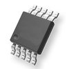
Part Details for LTC6911CMS-1#TRPBF by Linear Technology
Results Overview of LTC6911CMS-1#TRPBF by Linear Technology
- Distributor Offerings: (0 listings)
- Number of FFF Equivalents: (1 replacement)
- CAD Models: (Request Part)
- Number of Functional Equivalents: (1 option)
- Part Data Attributes: (Available)
- Reference Designs: (Not Available)
Tip: Data for a part may vary between manufacturers. You can filter for manufacturers on the top of the page next to the part image and part number.
LTC6911CMS-1#TRPBF Information
LTC6911CMS-1#TRPBF by Linear Technology is an Other Signal Circuit.
Other Signal Circuits are under the broader part category of Signal Circuits.
A signal is an electronic means of transmitting information, either as an analog signal with continuous values or a digital signal with discrete values. Signals are used in various systems and networks. Read more about Signal Circuits on our Signal Circuits part category page.
Part Details for LTC6911CMS-1#TRPBF
LTC6911CMS-1#TRPBF CAD Models
LTC6911CMS-1#TRPBF Part Data Attributes
|
|
LTC6911CMS-1#TRPBF
Linear Technology
Buy Now
Datasheet
|
Compare Parts:
LTC6911CMS-1#TRPBF
Linear Technology
LTC6911 - Dual Matched Amplifiers with Digitally Programmable Gain in MSOP; Package: MSOP; Pins: 10; Temperature Range: 0°C to 70°C
|
| Rohs Code | Yes | |
| Part Life Cycle Code | Transferred | |
| Ihs Manufacturer | LINEAR TECHNOLOGY CORP | |
| Part Package Code | MSOP | |
| Package Description | PLASTIC, MSOP-10 | |
| Pin Count | 10 | |
| Manufacturer Package Code | MS | |
| Reach Compliance Code | compliant | |
| HTS Code | 8542.39.00.01 | |
| Analog IC - Other Type | ANALOG CIRCUIT | |
| JESD-30 Code | S-PDSO-G10 | |
| JESD-609 Code | e3 | |
| Length | 3 mm | |
| Moisture Sensitivity Level | 1 | |
| Neg Supply Voltage-Max (Vsup) | -5.25 V | |
| Neg Supply Voltage-Min (Vsup) | -1.35 V | |
| Neg Supply Voltage-Nom (Vsup) | -5 V | |
| Number of Functions | 1 | |
| Number of Terminals | 10 | |
| Operating Temperature-Max | 85 °C | |
| Operating Temperature-Min | -40 °C | |
| Package Body Material | PLASTIC/EPOXY | |
| Package Code | TSSOP | |
| Package Shape | SQUARE | |
| Package Style | SMALL OUTLINE, THIN PROFILE, SHRINK PITCH | |
| Peak Reflow Temperature (Cel) | 260 | |
| Qualification Status | Not Qualified | |
| Seated Height-Max | 1.1 mm | |
| Supply Voltage-Max (Vsup) | 5.25 V | |
| Supply Voltage-Min (Vsup) | 1.35 V | |
| Supply Voltage-Nom (Vsup) | 5 V | |
| Surface Mount | YES | |
| Temperature Grade | INDUSTRIAL | |
| Terminal Finish | Matte Tin (Sn) | |
| Terminal Form | GULL WING | |
| Terminal Pitch | 0.5 mm | |
| Terminal Position | DUAL | |
| Time@Peak Reflow Temperature-Max (s) | 30 | |
| Width | 3 mm |
Alternate Parts for LTC6911CMS-1#TRPBF
This table gives cross-reference parts and alternative options found for LTC6911CMS-1#TRPBF. The Form Fit Function (FFF) tab will give you the options that are more likely to serve as direct pin-to-pin alternates or drop-in parts. The Functional Equivalents tab will give you options that are likely to match the same function of LTC6911CMS-1#TRPBF, but it may not fit your design. Always verify details of parts you are evaluating, as these parts are offered as suggestions for what you are looking for and are not guaranteed.
| Part Number | Manufacturer | Composite Price | Description | Compare |
|---|---|---|---|---|
| LTC6911CMS-1#TR | Analog Devices Inc | Check for Price | Analog Circuit, 1 Func, PDSO10 | LTC6911CMS-1#TRPBF vs LTC6911CMS-1#TR |
LTC6911CMS-1#TRPBF Frequently Asked Questions (FAQ)
-
A good PCB layout for the LTC6911CMS-1#TRPBF involves keeping the input and output traces short and separate, using a solid ground plane, and placing the device close to the power supply bypass capacitors. A 4-layer PCB with a dedicated ground plane is recommended.
-
The output capacitor should be chosen based on the desired output ripple voltage, output current, and operating frequency. A general rule of thumb is to use a capacitor with a value of at least 10uF and a voltage rating of 1.5 to 2 times the output voltage. X5R or X7R ceramic capacitors are recommended.
-
The maximum input voltage that can be applied to the LTC6911CMS-1#TRPBF is 15V, but it's recommended to operate the device within the specified input voltage range of 2.7V to 12V for optimal performance and reliability.
-
The LTC6911CMS-1#TRPBF has a SYNC pin that can be used to synchronize the switching frequency with other switching regulators. The SYNC pin can be connected to a clock signal or another regulator's SYNC pin to achieve synchronization.
-
The thermal derating of the LTC6911CMS-1#TRPBF is typically 50% at 85°C and 75% at 105°C. This means that the maximum output current of the device will be reduced at higher temperatures to prevent overheating. The actual output current should be derated based on the operating temperature and the thermal resistance of the package.
