-
Part Symbol
-
Footprint
-
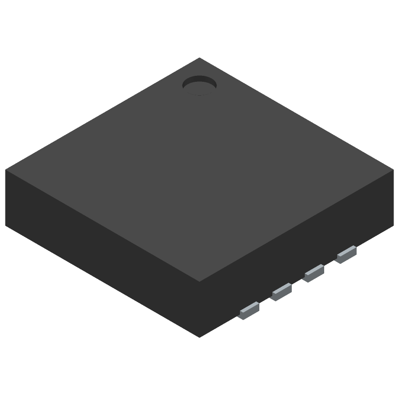
3D Model
Available Download Formats
By downloading CAD models, you agree to our Terms & Conditions and Privacy Policy
Precision, Low Power Rail-to-Rail Input/Output Differential Op Amp/SAR ADC Driver
Tip: Data for a part may vary between manufacturers. You can filter for manufacturers on the top of the page next to the part image and part number.
LTC6362IDD#PBF by Analog Devices Inc is an Other Signal Circuit.
Other Signal Circuits are under the broader part category of Signal Circuits.
A signal is an electronic means of transmitting information, either as an analog signal with continuous values or a digital signal with discrete values. Signals are used in various systems and networks. Read more about Signal Circuits on our Signal Circuits part category page.
| Part # | Distributor | Description | Stock | Price | Buy | |
|---|---|---|---|---|---|---|
|
DISTI #
4019129
|
Farnell | DIFF-AMP, 180MHZ, -40 TO 85DEG C, DFN-8 RoHS: Compliant Min Qty: 1 Lead time: 11 Weeks, 1 Days Container: Each | 35 |
|
$3.0200 / $6.0533 | Buy Now |
|
DISTI #
V36:1790_06491496
|
Arrow Electronics | SP Amp DIFF AMP Single R-R I/O ±2.625V/5.25V 8-Pin DFN EP Tube RoHS: Compliant Min Qty: 121 Package Multiple: 121 Lead time: 10 Weeks Date Code: 2449 | Americas - 82 |
|
$2.8782 | Buy Now |
|
DISTI #
87796027
|
Verical | SP Amp DIFF AMP Single R-R I/O ±2.625V/5.25V 8-Pin DFN EP Tube RoHS: Compliant Min Qty: 82 Package Multiple: 82 Date Code: 2449 | Americas - 82 |
|
$2.8782 | Buy Now |
By downloading CAD models, you agree to our Terms & Conditions and Privacy Policy
|
|
LTC6362IDD#PBF
Analog Devices Inc
Buy Now
Datasheet
|
Compare Parts:
LTC6362IDD#PBF
Analog Devices Inc
Precision, Low Power Rail-to-Rail Input/Output Differential Op Amp/SAR ADC Driver
|
| Pbfree Code | No | |
| Rohs Code | Yes | |
| Part Life Cycle Code | Obsolete | |
| Ihs Manufacturer | ANALOG DEVICES INC | |
| Package Description | 3 X 3 MM, LEAD FREE, PLASTIC, MO-229WEED-1, DFN-8 | |
| Pin Count | 8 | |
| Manufacturer Package Code | 05-08-1698 | |
| Reach Compliance Code | compliant | |
| ECCN Code | EAR99 | |
| HTS Code | 8542.33.00.01 | |
| Samacsys Manufacturer | Analog Devices | |
| Analog IC - Other Type | ANALOG CIRCUIT | |
| JESD-30 Code | S-PDSO-N8 | |
| JESD-609 Code | e3 | |
| Length | 3 mm | |
| Moisture Sensitivity Level | 1 | |
| Number of Functions | 1 | |
| Number of Terminals | 8 | |
| Operating Temperature-Max | 85 °C | |
| Operating Temperature-Min | -40 °C | |
| Package Body Material | PLASTIC/EPOXY | |
| Package Code | HVSON | |
| Package Shape | SQUARE | |
| Package Style | SMALL OUTLINE, HEAT SINK/SLUG, VERY THIN PROFILE | |
| Peak Reflow Temperature (Cel) | 260 | |
| Seated Height-Max | 0.8 mm | |
| Supply Voltage-Max (Vsup) | 5.25 V | |
| Supply Voltage-Min (Vsup) | 2.8 V | |
| Supply Voltage-Nom (Vsup) | 3 V | |
| Surface Mount | YES | |
| Technology | CMOS | |
| Temperature Grade | INDUSTRIAL | |
| Terminal Finish | Matte Tin (Sn) | |
| Terminal Form | NO LEAD | |
| Terminal Pitch | 0.5 mm | |
| Terminal Position | DUAL | |
| Time@Peak Reflow Temperature-Max (s) | 30 | |
| Width | 3 mm |
This table gives cross-reference parts and alternative options found for LTC6362IDD#PBF. The Form Fit Function (FFF) tab will give you the options that are more likely to serve as direct pin-to-pin alternates or drop-in parts. The Functional Equivalents tab will give you options that are likely to match the same function of LTC6362IDD#PBF, but it may not fit your design. Always verify details of parts you are evaluating, as these parts are offered as suggestions for what you are looking for and are not guaranteed.
| Part Number | Manufacturer | Composite Price | Description | Compare |
|---|---|---|---|---|
| LTC6362IMS8#TRPBF | Analog Devices Inc | Check for Price | Precision, Low Power Rail-to-Rail Input/Output Differential Op Amp/SAR ADC Driver | LTC6362IDD#PBF vs LTC6362IMS8#TRPBF |
| LTC6362CMS8#PBF | Analog Devices Inc | Check for Price | Precision, Low Power Rail-to-Rail Input/Output Differential Op Amp/SAR ADC Driver | LTC6362IDD#PBF vs LTC6362CMS8#PBF |
| LTC6362HMS8#PBF | Analog Devices Inc | Check for Price | Precision, Low Power Rail-to-Rail Input/Output Differential Op Amp/SAR ADC Driver | LTC6362IDD#PBF vs LTC6362HMS8#PBF |
A good PCB layout for the LTC6362IDD#PBF involves keeping the input and output traces separate, using a solid ground plane, and placing the device close to the input and output connectors. Additionally, it's recommended to use a low-ESR capacitor for the VCC bypass and to keep the analog and digital grounds separate.
To optimize the gain and bandwidth of the LTC6362IDD#PBF, you can adjust the gain resistors (R1 and R2) and the compensation capacitor (Ccomp). A higher gain resistor value will increase the gain, while a lower value will decrease it. The compensation capacitor value will affect the bandwidth, with a larger value increasing the bandwidth.
The maximum input voltage that the LTC6362IDD#PBF can handle is 6V, which is the absolute maximum rating. However, it's recommended to keep the input voltage within the recommended operating range of 2.7V to 5.5V to ensure optimal performance and reliability.
To ensure that the LTC6362IDD#PBF is operating within its recommended operating conditions, you should monitor the device's temperature, input voltage, and output current. The device should be operated within the recommended temperature range of -40°C to 125°C, with an input voltage between 2.7V and 5.5V, and an output current not exceeding 100mA.
The LTC6362IDD#PBF has a thermal pad that should be connected to a solid ground plane to ensure proper heat dissipation. You should also ensure that the device is mounted on a PCB with a good thermal conductivity, and that there is adequate airflow around the device to prevent overheating.