-
Part Symbol
-
Footprint
-
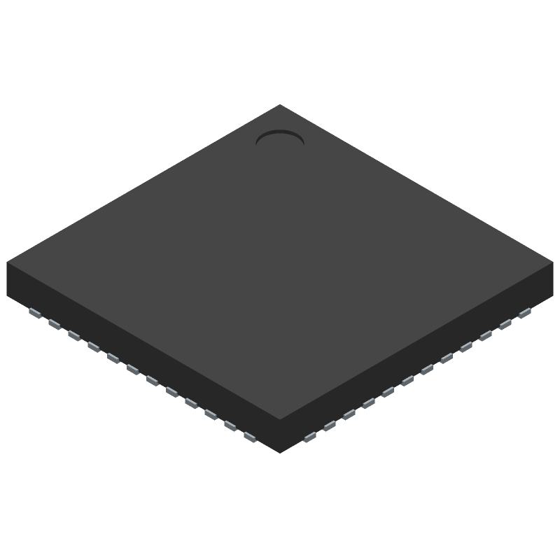
3D Model
Available Download Formats
By downloading CAD models, you agree to our Terms & Conditions and Privacy Policy
16-Bit, 20Msps Low Power ADC
Tip: Data for a part may vary between manufacturers. You can filter for manufacturers on the top of the page next to the part image and part number.
LTC2159CUK#PBF by Analog Devices Inc is an Analog to Digital Converter.
Analog to Digital Converters are under the broader part category of Converters.
A converter is an electrical circuit that transforms electric energy into a different form that will support a elecrical load needed by a device. Read more about Converters on our Converters part category page.
| Part # | Distributor | Description | Stock | Price | Buy | |
|---|---|---|---|---|---|---|
|
DISTI #
505-LTC2159CUK#PBF-ND
|
DigiKey | IC ADC 16BIT PIPELINED 48QFN Min Qty: 52 Lead time: 20 Weeks Container: Tube | Temporarily Out of Stock |
|
$40.2125 | Buy Now |
|
DISTI #
584-LTC2159CUK#PBF
|
Mouser Electronics | Analog to Digital Converters - ADC 16-B, 20Msps L Pwr ADC RoHS: Compliant | 0 |
|
$40.2100 / $40.2200 | Order Now |
|
|
Analog Devices Inc | 16-B, 20Msps L Pwr ADC Package Multiple: 52 | 1144 |
|
$32.1700 / $45.8500 | Buy Now |
|
DISTI #
43241098
|
Verical | 1-Channel Single ADC Pipelined 20Msps 16-bit Parallel 48-Pin QFN EP Tube RoHS: Compliant Min Qty: 52 Package Multiple: 52 | Americas - 1144 |
|
$39.7897 | Buy Now |
|
DISTI #
LTC2159CUK#PBF
|
Richardson RFPD | CONVERTER - ADC RoHS: Compliant Min Qty: 52 | 0 |
|
$41.5300 / $48.2600 | Buy Now |
By downloading CAD models, you agree to our Terms & Conditions and Privacy Policy
|
|
LTC2159CUK#PBF
Analog Devices Inc
Buy Now
Datasheet
|
Compare Parts:
LTC2159CUK#PBF
Analog Devices Inc
16-Bit, 20Msps Low Power ADC
|
| Pbfree Code | No | |
| Rohs Code | Yes | |
| Part Life Cycle Code | Active | |
| Ihs Manufacturer | ANALOG DEVICES INC | |
| Package Description | 7 X 7 MM, LEAD FREE, PLASTIC, MO-220WKKD-2, QFN-48 | |
| Pin Count | 48 | |
| Manufacturer Package Code | 05-08-1704 | |
| Reach Compliance Code | compliant | |
| Samacsys Manufacturer | Analog Devices | |
| Analog Input Voltage-Max | 2 V | |
| Analog Input Voltage-Min | -2 V | |
| Converter Type | ADC, PROPRIETARY METHOD | |
| JESD-30 Code | S-PQCC-N48 | |
| JESD-609 Code | e3 | |
| Length | 7 mm | |
| Linearity Error-Max (EL) | 0.0092% | |
| Moisture Sensitivity Level | 1 | |
| Number of Analog In Channels | 1 | |
| Number of Bits | 16 | |
| Number of Functions | 1 | |
| Number of Terminals | 48 | |
| Operating Temperature-Max | 70 °C | |
| Operating Temperature-Min | ||
| Output Bit Code | OFFSET BINARY, 2'S COMPLEMENT BINARY | |
| Output Format | PARALLEL, WORD | |
| Package Body Material | PLASTIC/EPOXY | |
| Package Code | HVQCCN | |
| Package Shape | SQUARE | |
| Package Style | CHIP CARRIER, HEAT SINK/SLUG, VERY THIN PROFILE | |
| Peak Reflow Temperature (Cel) | 260 | |
| Sample Rate | 20 MHz | |
| Sample and Hold / Track and Hold | SAMPLE | |
| Seated Height-Max | 0.8 mm | |
| Supply Voltage-Nom | 1.8 V | |
| Surface Mount | YES | |
| Technology | CMOS | |
| Temperature Grade | COMMERCIAL | |
| Terminal Finish | Matte Tin (Sn) | |
| Terminal Form | NO LEAD | |
| Terminal Pitch | 0.5 mm | |
| Terminal Position | QUAD | |
| Time@Peak Reflow Temperature-Max (s) | 30 | |
| Width | 7 mm |
This table gives cross-reference parts and alternative options found for LTC2159CUK#PBF. The Form Fit Function (FFF) tab will give you the options that are more likely to serve as direct pin-to-pin alternates or drop-in parts. The Functional Equivalents tab will give you options that are likely to match the same function of LTC2159CUK#PBF, but it may not fit your design. Always verify details of parts you are evaluating, as these parts are offered as suggestions for what you are looking for and are not guaranteed.
| Part Number | Manufacturer | Composite Price | Description | Compare |
|---|---|---|---|---|
| LTC2159CUK#PBF | Linear Technology | Check for Price | LTC2159 - 16-Bit, 20Msps Low Power ADC; Package: QFN; Pins: 48; Temperature Range: 0°C to 70°C | LTC2159CUK#PBF vs LTC2159CUK#PBF |
| LTC2159CUK#TRPBF | Linear Technology | Check for Price | LTC2159 - 16-Bit, 20Msps Low Power ADC; Package: QFN; Pins: 48; Temperature Range: 0°C to 70°C | LTC2159CUK#PBF vs LTC2159CUK#TRPBF |
| LTC2159IUK#TRPBF | Linear Technology | Check for Price | LTC2159 - 16-Bit, 20Msps Low Power ADC; Package: QFN; Pins: 48; Temperature Range: -40°C to 85°C | LTC2159CUK#PBF vs LTC2159IUK#TRPBF |
| LTC2159IUK#PBF | Linear Technology | Check for Price | LTC2159 - 16-Bit, 20Msps Low Power ADC; Package: QFN; Pins: 48; Temperature Range: -40°C to 85°C | LTC2159CUK#PBF vs LTC2159IUK#PBF |
A good PCB layout for the LTC2159 involves keeping the analog and digital grounds separate, using a solid ground plane, and minimizing the length of the traces between the ADC and the analog input pins. Additionally, it's recommended to use a low-ESR capacitor for the VCC pin and to decouple the VCC pin with a 0.1uF capacitor.
To ensure accurate conversion results, it's essential to follow proper PCB layout guidelines, use a high-quality analog input signal, and ensure that the ADC is properly calibrated. Additionally, the LTC2159 has a built-in calibration feature that can be used to compensate for any internal errors.
The maximum sampling rate of the LTC2159 is 135Msps, but this can be limited by the specific application and the quality of the analog input signal. It's recommended to consult the datasheet and application notes for more information on achieving the highest possible sampling rate.
Yes, the LTC2159 can be used in a multi-channel application by using multiple devices or by using a multiplexer to switch between multiple analog input channels. However, it's essential to ensure that the multiplexer is properly designed and that the switching time is minimized to avoid any errors or distortions in the conversion results.
The LTC2159 has a parallel output interface that can be easily interfaced with a microcontroller or FPGA. The specific interface requirements will depend on the particular microcontroller or FPGA being used, but generally, it involves connecting the output pins of the LTC2159 to the input pins of the microcontroller or FPGA and using a clock signal to synchronize the data transfer.