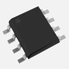
Part Details for LTC1864ACMS8#PBF by Linear Technology
Results Overview of LTC1864ACMS8#PBF by Linear Technology
- Distributor Offerings: (2 listings)
- Number of FFF Equivalents: (0 replacements)
- CAD Models: (Request Part)
- Number of Functional Equivalents: (1 option)
- Part Data Attributes: (Available)
- Reference Designs: (Not Available)
Tip: Data for a part may vary between manufacturers. You can filter for manufacturers on the top of the page next to the part image and part number.
LTC1864ACMS8#PBF Information
LTC1864ACMS8#PBF by Linear Technology is an Analog to Digital Converter.
Analog to Digital Converters are under the broader part category of Converters.
A converter is an electrical circuit that transforms electric energy into a different form that will support a elecrical load needed by a device. Read more about Converters on our Converters part category page.
Price & Stock for LTC1864ACMS8#PBF
| Part # | Distributor | Description | Stock | Price | Buy | |
|---|---|---|---|---|---|---|
|
|
Vyrian | Converters | 607 |
|
RFQ | |
|
|
Win Source Electronics | IC A/D CONV 1CH 16BIT 8-MSOP / 1-Channel Single ADC SAR 250ksps 16-bit Serial Automotive 8-Pin MSOP Tube | 5000 |
|
$26.1134 / $39.1695 | Buy Now |
Part Details for LTC1864ACMS8#PBF
LTC1864ACMS8#PBF CAD Models
LTC1864ACMS8#PBF Part Data Attributes
|
|
LTC1864ACMS8#PBF
Linear Technology
Buy Now
Datasheet
|
Compare Parts:
LTC1864ACMS8#PBF
Linear Technology
LTC1864 - µPower, 16-Bit, 250ksps 1- and 2-Channel ADCs in SOIC; Package: MSOP; Pins: 8; Temperature Range: 0°C to 70°C
|
| Rohs Code | Yes | |
| Part Life Cycle Code | Transferred | |
| Ihs Manufacturer | LINEAR TECHNOLOGY CORP | |
| Part Package Code | MSOP | |
| Package Description | LEAD FREE, PLASTIC, MSOP-8 | |
| Pin Count | 8 | |
| Manufacturer Package Code | MS8 | |
| Reach Compliance Code | compliant | |
| HTS Code | 8542.39.00.01 | |
| Analog Input Voltage-Max | 5.25 V | |
| Analog Input Voltage-Min | ||
| Conversion Time-Max | 3.2 µs | |
| Converter Type | ADC, SUCCESSIVE APPROXIMATION | |
| JESD-30 Code | S-PDSO-G8 | |
| JESD-609 Code | e3 | |
| Length | 3 mm | |
| Linearity Error-Max (EL) | 0.0092% | |
| Moisture Sensitivity Level | 1 | |
| Number of Analog In Channels | 1 | |
| Number of Bits | 16 | |
| Number of Functions | 1 | |
| Number of Terminals | 8 | |
| Operating Temperature-Max | 70 °C | |
| Operating Temperature-Min | ||
| Output Bit Code | BINARY | |
| Output Format | SERIAL | |
| Package Body Material | PLASTIC/EPOXY | |
| Package Code | TSSOP | |
| Package Equivalence Code | TSSOP8,.19 | |
| Package Shape | SQUARE | |
| Package Style | SMALL OUTLINE, THIN PROFILE, SHRINK PITCH | |
| Peak Reflow Temperature (Cel) | 260 | |
| Qualification Status | Not Qualified | |
| Sample Rate | 0.25 MHz | |
| Sample and Hold / Track and Hold | SAMPLE | |
| Seated Height-Max | 1.1 mm | |
| Supply Voltage-Nom | 5 V | |
| Surface Mount | YES | |
| Technology | CMOS | |
| Temperature Grade | COMMERCIAL | |
| Terminal Finish | Matte Tin (Sn) | |
| Terminal Form | GULL WING | |
| Terminal Pitch | 0.65 mm | |
| Terminal Position | DUAL | |
| Time@Peak Reflow Temperature-Max (s) | 30 | |
| Width | 3 mm |
Alternate Parts for LTC1864ACMS8#PBF
This table gives cross-reference parts and alternative options found for LTC1864ACMS8#PBF. The Form Fit Function (FFF) tab will give you the options that are more likely to serve as direct pin-to-pin alternates or drop-in parts. The Functional Equivalents tab will give you options that are likely to match the same function of LTC1864ACMS8#PBF, but it may not fit your design. Always verify details of parts you are evaluating, as these parts are offered as suggestions for what you are looking for and are not guaranteed.
| Part Number | Manufacturer | Composite Price | Description | Compare |
|---|---|---|---|---|
| LTC1864CMS8#PBF | Analog Devices Inc | $7.2067 | µPower, 16-Bit, 250ksps 1- and 2-Channel ADCs in SOIC | LTC1864ACMS8#PBF vs LTC1864CMS8#PBF |
LTC1864ACMS8#PBF Frequently Asked Questions (FAQ)
-
The maximum operating temperature range for the LTC1864 is -40°C to 125°C.
-
To ensure accurate voltage measurements, make sure to use a low-noise, low-impedance voltage source, and ensure that the input voltage is within the specified range. Also, use a high-precision voltage reference and a low-drift amplifier to minimize errors.
-
For optimal performance, use a 4-layer PCB with a solid ground plane, and keep the analog and digital signals separate. Use short, direct traces for the input and output signals, and avoid crossing digital and analog signals.
-
To minimize EMI and RFI, use a shielded enclosure, and ensure that the PCB is properly grounded. Use EMI filters and shielding on the input and output lines, and consider using a common-mode choke to reduce noise.
-
The recommended power-up sequence for the LTC1864 is to power up the analog supply (VCC) first, followed by the digital supply (VDD). This ensures that the analog circuitry is powered up before the digital circuitry.
