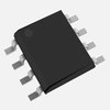
Part Details for LT1012AIS8#PBF by Linear Technology
Results Overview of LT1012AIS8#PBF by Linear Technology
- Distributor Offerings: (0 listings)
- Number of FFF Equivalents: (2 replacements)
- CAD Models: (Request Part)
- Number of Functional Equivalents: (10 options)
- Part Data Attributes: (Available)
- Reference Designs: (Not Available)
Tip: Data for a part may vary between manufacturers. You can filter for manufacturers on the top of the page next to the part image and part number.
LT1012AIS8#PBF Information
LT1012AIS8#PBF by Linear Technology is an Operational Amplifier.
Operational Amplifiers are under the broader part category of Amplifier Circuits.
Amplifier circuits use external power to increase the amplitude of an input signal. They can be used to perform linear amplifications or logarithmic functions. Read more about Amplifier Circuits on our Amplifier Circuits part category page.
Part Details for LT1012AIS8#PBF
LT1012AIS8#PBF CAD Models
LT1012AIS8#PBF Part Data Attributes
|
|
LT1012AIS8#PBF
Linear Technology
Buy Now
Datasheet
|
Compare Parts:
LT1012AIS8#PBF
Linear Technology
LT1012 - Picoamp Input Current, Microvolt Offset, Low Noise Op Amp; Package: SO; Pins: 8; Temperature Range: -40°C to 85°C
|
| Rohs Code | Yes | |
| Part Life Cycle Code | Transferred | |
| Ihs Manufacturer | LINEAR TECHNOLOGY CORP | |
| Part Package Code | SOIC | |
| Package Description | 0.150 INCH, LEAD FREE, PLASTIC, SOP-8 | |
| Pin Count | 8 | |
| Manufacturer Package Code | S8 | |
| Reach Compliance Code | compliant | |
| ECCN Code | EAR99 | |
| HTS Code | 8542.33.00.01 | |
| Amplifier Type | OPERATIONAL AMPLIFIER | |
| Architecture | VOLTAGE-FEEDBACK | |
| Average Bias Current-Max (IIB) | 0.0008 µA | |
| Bias Current-Max (IIB) @25C | 0.00015 µA | |
| Common-mode Reject Ratio-Nom | 128 dB | |
| Frequency Compensation | YES | |
| Input Offset Voltage-Max | 180 µV | |
| JESD-30 Code | R-PDSO-G8 | |
| JESD-609 Code | e3 | |
| Length | 4.9025 mm | |
| Low-Bias | YES | |
| Low-Offset | YES | |
| Micropower | YES | |
| Moisture Sensitivity Level | 1 | |
| Neg Supply Voltage Limit-Max | -20 V | |
| Neg Supply Voltage-Nom (Vsup) | -15 V | |
| Number of Functions | 1 | |
| Number of Terminals | 8 | |
| Operating Temperature-Max | 85 °C | |
| Operating Temperature-Min | -40 °C | |
| Package Body Material | PLASTIC/EPOXY | |
| Package Code | SOP | |
| Package Equivalence Code | SOP8,.25 | |
| Package Shape | RECTANGULAR | |
| Package Style | SMALL OUTLINE | |
| Peak Reflow Temperature (Cel) | 260 | |
| Qualification Status | Not Qualified | |
| Seated Height-Max | 1.752 mm | |
| Slew Rate-Min | 0.1 V/us | |
| Slew Rate-Nom | 0.2 V/us | |
| Supply Current-Max | 0.6 mA | |
| Supply Voltage Limit-Max | 20 V | |
| Supply Voltage-Nom (Vsup) | 15 V | |
| Surface Mount | YES | |
| Technology | BIPOLAR | |
| Temperature Grade | INDUSTRIAL | |
| Terminal Finish | Matte Tin (Sn) | |
| Terminal Form | GULL WING | |
| Terminal Pitch | 1.27 mm | |
| Terminal Position | DUAL | |
| Time@Peak Reflow Temperature-Max (s) | 30 | |
| Voltage Gain-Min | 200000 | |
| Width | 3.899 mm |
Alternate Parts for LT1012AIS8#PBF
This table gives cross-reference parts and alternative options found for LT1012AIS8#PBF. The Form Fit Function (FFF) tab will give you the options that are more likely to serve as direct pin-to-pin alternates or drop-in parts. The Functional Equivalents tab will give you options that are likely to match the same function of LT1012AIS8#PBF, but it may not fit your design. Always verify details of parts you are evaluating, as these parts are offered as suggestions for what you are looking for and are not guaranteed.
| Part Number | Manufacturer | Composite Price | Description | Compare |
|---|---|---|---|---|
| LT1012AIS8#PBF | Analog Devices Inc | $5.2991 | Picoamp Input Current, Microvolt Offset, Low Noise Op Amp | LT1012AIS8#PBF vs LT1012AIS8#PBF |
| LT1012AIS8#TRPBF | Analog Devices Inc | Check for Price | Picoamp Input Current, Microvolt Offset, Low Noise Op Amp | LT1012AIS8#PBF vs LT1012AIS8#TRPBF |
LT1012AIS8#PBF Frequently Asked Questions (FAQ)
-
A good PCB layout for the LT1012AIS8 involves keeping the input and output traces short and separate, using a solid ground plane, and placing the bypass capacitors close to the device. A 4-layer PCB with a dedicated power plane and a dedicated ground plane is recommended.
-
To ensure stability, make sure to follow the recommended compensation network, use a minimum output capacitance of 10uF, and avoid capacitive loads. Also, ensure that the device is operated within its recommended operating conditions and that the input voltage is well-regulated.
-
The maximum power dissipation of the LT1012AIS8 is dependent on the package and the ambient temperature. For the IS8 package, the maximum power dissipation is 1.4W at 25°C ambient temperature. However, it is recommended to derate the power dissipation based on the ambient temperature and the thermal resistance of the package.
-
The LT1012AIS8 is rated for operation up to 125°C junction temperature. However, the device's performance and reliability may degrade at high temperatures. It is recommended to derate the power dissipation and ensure proper heat sinking to maintain a safe junction temperature.
-
To protect the LT1012AIS8 from input voltage transients, use a TVS diode or a transient voltage suppressor at the input. Also, ensure that the input voltage is well-regulated and that the device is operated within its recommended operating conditions.
