-
Part Symbol
-
Footprint
-
3D Model
Available Download Formats
By downloading CAD models, you agree to our Terms & Conditions and Privacy Policy

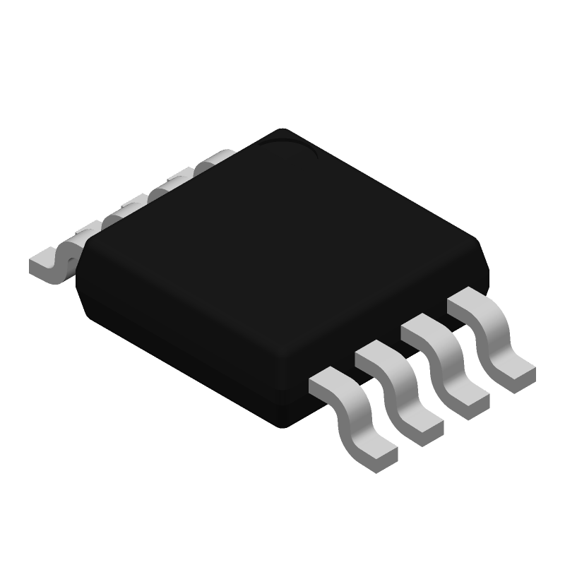
370MHz, Differential, High Speed Op Amp 8-VSSOP -40 to 85
Tip: Data for a part may vary between manufacturers. You can filter for manufacturers on the top of the page next to the part image and part number.
LMH6551MM by Texas Instruments is an Operational Amplifier.
Operational Amplifiers are under the broader part category of Amplifier Circuits.
Amplifier circuits use external power to increase the amplitude of an input signal. They can be used to perform linear amplifications or logarithmic functions. Read more about Amplifier Circuits on our Amplifier Circuits part category page.
| Part # | Distributor | Description | Stock | Price | Buy | |
|---|---|---|---|---|---|---|
|
|
Vyrian | Peripheral ICs | 1371 |
|
RFQ | |
|
|
Win Source Electronics | IC OPAMP VFB 370MHZ 8VSSOP | 4638 |
|
$2.1760 / $3.2640 | Buy Now |
By downloading CAD models, you agree to our Terms & Conditions and Privacy Policy
|
|
LMH6551MM
Texas Instruments
Buy Now
Datasheet
|
Compare Parts:
LMH6551MM
Texas Instruments
370MHz, Differential, High Speed Op Amp 8-VSSOP -40 to 85
|
| Pbfree Code | Yes | |
| Rohs Code | No | |
| Part Life Cycle Code | Obsolete | |
| Ihs Manufacturer | TEXAS INSTRUMENTS INC | |
| Part Package Code | MSOP | |
| Package Description | MSOP-8 | |
| Pin Count | 8 | |
| Reach Compliance Code | not_compliant | |
| ECCN Code | EAR99 | |
| HTS Code | 8542.33.00.01 | |
| Samacsys Manufacturer | Texas Instruments | |
| Amplifier Type | OPERATIONAL AMPLIFIER | |
| Architecture | VOLTAGE-FEEDBACK | |
| Average Bias Current-Max (IIB) | 10 µA | |
| Bandwidth (3dB)-Nom | 300 MHz | |
| Bias Current-Max (IIB) @25C | 10 µA | |
| Common-mode Reject Ratio-Min | 72 dB | |
| Common-mode Reject Ratio-Nom | 80 dB | |
| Frequency Compensation | YES | |
| Input Offset Voltage-Max | 5000 µV | |
| JESD-30 Code | S-PDSO-G8 | |
| JESD-609 Code | e0 | |
| Length | 3 mm | |
| Low-Bias | NO | |
| Low-Offset | NO | |
| Micropower | NO | |
| Moisture Sensitivity Level | 1 | |
| Neg Supply Voltage Limit-Max | -6.6 V | |
| Neg Supply Voltage-Nom (Vsup) | -5 V | |
| Number of Functions | 1 | |
| Number of Terminals | 8 | |
| Operating Temperature-Max | 85 °C | |
| Operating Temperature-Min | -40 °C | |
| Package Body Material | PLASTIC/EPOXY | |
| Package Code | TSSOP | |
| Package Equivalence Code | TSSOP8,.19 | |
| Package Shape | SQUARE | |
| Package Style | SMALL OUTLINE, THIN PROFILE, SHRINK PITCH | |
| Packing Method | TR | |
| Peak Reflow Temperature (Cel) | 260 | |
| Power | NO | |
| Programmable Power | NO | |
| Qualification Status | Not Qualified | |
| Seated Height-Max | 1.09 mm | |
| Slew Rate-Nom | 2400 V/us | |
| Supply Current-Max | 14.5 mA | |
| Supply Voltage Limit-Max | 6.6 V | |
| Supply Voltage-Nom (Vsup) | 5 V | |
| Surface Mount | YES | |
| Temperature Grade | INDUSTRIAL | |
| Terminal Finish | Tin/Lead (Sn/Pb) | |
| Terminal Form | GULL WING | |
| Terminal Pitch | 0.65 mm | |
| Terminal Position | DUAL | |
| Unity Gain BW-Nom | 370000 | |
| Wideband | YES | |
| Width | 3 mm |
Texas Instruments provides a recommended PCB layout in the application note SLWA043, which includes guidelines for component placement, routing, and grounding to minimize noise and ensure optimal performance.
The choice of input and output capacitors depends on the specific application and operating conditions. TI recommends using low-ESR capacitors with a minimum capacitance of 10uF for the input and output. The application note SLWA043 provides more detailed guidance on capacitor selection.
The LMH6551MM is rated for operation from -40°C to 85°C. However, the device may be able to operate beyond this range with reduced performance and reliability. Consult the datasheet and application notes for more information on temperature-related performance and limitations.
To ensure EMC, follow proper PCB layout and design practices, such as using a solid ground plane, minimizing loop areas, and using shielding and filtering as needed. TI also provides guidance on EMC in the application note SLWA043.
The recommended power-up sequence is to apply the power supply voltage (VCC) before applying the input signal. This ensures that the device is properly biased and configured before signal processing begins.