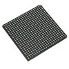
Part Details for LFEC15E-3FN484C by Lattice Semiconductor Corporation
Results Overview of LFEC15E-3FN484C by Lattice Semiconductor Corporation
- Distributor Offerings: (0 listings)
- Number of FFF Equivalents: (2 replacements)
- CAD Models: (Request Part)
- Number of Functional Equivalents: (10 options)
- Part Data Attributes: (Available)
- Reference Designs: (Not Available)
Tip: Data for a part may vary between manufacturers. You can filter for manufacturers on the top of the page next to the part image and part number.
LFEC15E-3FN484C Information
LFEC15E-3FN484C by Lattice Semiconductor Corporation is a Field Programmable Gate Array.
Field Programmable Gate Arrays are under the broader part category of Programmable Logic Devices.
Programmable Logic Devices (PLDs) are reconfigurable digital components that can be customized for different applications, offering flexibility and improved performance over fixed logic devices. Read more about Programmable Logic Devices on our Programmable Logic part category page.
Part Details for LFEC15E-3FN484C
LFEC15E-3FN484C CAD Models
LFEC15E-3FN484C Part Data Attributes
|
|
LFEC15E-3FN484C
Lattice Semiconductor Corporation
Buy Now
Datasheet
|
Compare Parts:
LFEC15E-3FN484C
Lattice Semiconductor Corporation
Field Programmable Gate Array, 1920 CLBs, 420MHz, 15300-Cell, PBGA484, 23 X 23 MM, 1 MM PITCH, LEAD FREE, PLASTIC, FPBGA-484
|
| Pbfree Code | Yes | |
| Rohs Code | Yes | |
| Part Life Cycle Code | Obsolete | |
| Ihs Manufacturer | LATTICE SEMICONDUCTOR CORP | |
| Part Package Code | BGA | |
| Package Description | 23 X 23 MM, 1 MM PITCH, LEAD FREE, PLASTIC, FPBGA-484 | |
| Pin Count | 484 | |
| Reach Compliance Code | compliant | |
| ECCN Code | 3A991.D | |
| HTS Code | 8542.39.00.01 | |
| Clock Frequency-Max | 420 MHz | |
| Combinatorial Delay of a CLB-Max | 0.56 ns | |
| JESD-30 Code | S-PBGA-B484 | |
| JESD-609 Code | e1 | |
| Length | 23 mm | |
| Moisture Sensitivity Level | 3 | |
| Number of CLBs | 1920 | |
| Number of Inputs | 352 | |
| Number of Logic Cells | 15300 | |
| Number of Outputs | 352 | |
| Number of Terminals | 484 | |
| Operating Temperature-Max | 85 °C | |
| Operating Temperature-Min | ||
| Organization | 1920 CLBS | |
| Package Body Material | PLASTIC/EPOXY | |
| Package Code | BGA | |
| Package Equivalence Code | BGA484,22X22,40 | |
| Package Shape | SQUARE | |
| Package Style | GRID ARRAY | |
| Peak Reflow Temperature (Cel) | 250 | |
| Programmable Logic Type | FIELD PROGRAMMABLE GATE ARRAY | |
| Qualification Status | Not Qualified | |
| Seated Height-Max | 2.6 mm | |
| Supply Voltage-Max | 1.26 V | |
| Supply Voltage-Min | 1.14 V | |
| Supply Voltage-Nom | 1.2 V | |
| Surface Mount | YES | |
| Temperature Grade | OTHER | |
| Terminal Finish | Tin/Silver/Copper (Sn/Ag/Cu) | |
| Terminal Form | BALL | |
| Terminal Pitch | 1 mm | |
| Terminal Position | BOTTOM | |
| Time@Peak Reflow Temperature-Max (s) | 40 | |
| Width | 23 mm |
Alternate Parts for LFEC15E-3FN484C
This table gives cross-reference parts and alternative options found for LFEC15E-3FN484C. The Form Fit Function (FFF) tab will give you the options that are more likely to serve as direct pin-to-pin alternates or drop-in parts. The Functional Equivalents tab will give you options that are likely to match the same function of LFEC15E-3FN484C, but it may not fit your design. Always verify details of parts you are evaluating, as these parts are offered as suggestions for what you are looking for and are not guaranteed.
| Part Number | Manufacturer | Composite Price | Description | Compare |
|---|---|---|---|---|
| LFEC15E-3F484C | Lattice Semiconductor Corporation | Check for Price | Field Programmable Gate Array, 1920 CLBs, 420MHz, 15300-Cell, PBGA484, 23 X 23 MM, 1 MM PITCH, PLASTIC, FPBGA-484 | LFEC15E-3FN484C vs LFEC15E-3F484C |
| LFEC15E-3FN484I | Lattice Semiconductor Corporation | Check for Price | Field Programmable Gate Array, 1920 CLBs, 420MHz, 15300-Cell, PBGA484, 23 X 23 MM, 1 MM PITCH, LEAD FREE, PLASTIC, FPBGA-484 | LFEC15E-3FN484C vs LFEC15E-3FN484I |
LFEC15E-3FN484C Frequently Asked Questions (FAQ)
-
Lattice Semiconductor provides a PCB layout guide and reference design files for the LFEC15E-3FN484C, which can be found on their website. It's recommended to follow these guidelines to ensure optimal performance and minimize signal integrity issues.
-
The LFEC15E-3FN484C requires a specific power-up and power-down sequence to ensure proper operation. Lattice Semiconductor recommends following the power management guidelines in the datasheet, and using a power management IC (PMIC) to sequence the power rails correctly.
-
The LFEC15E-3FN484C has a maximum junction temperature of 125°C. To ensure reliable operation, it's essential to implement proper thermal management, such as using a heat sink, thermal interface material, and ensuring good airflow around the device.
-
Lattice Semiconductor provides a range of tools and resources, including the Lattice Diamond design software, to help optimize the LFEC15E-3FN484C for specific applications. Engineers can use these tools to optimize the device's configuration, clocking, and routing for their particular use case.
-
The LFEC15E-3FN484C is not specifically designed for radiation-tolerant or high-reliability applications. However, Lattice Semiconductor provides information on the device's radiation tolerance and reliability characteristics in the datasheet and application notes. Engineers should consult these resources to determine if the device is suitable for their specific application.
