-
Part Symbol
-
Footprint
-
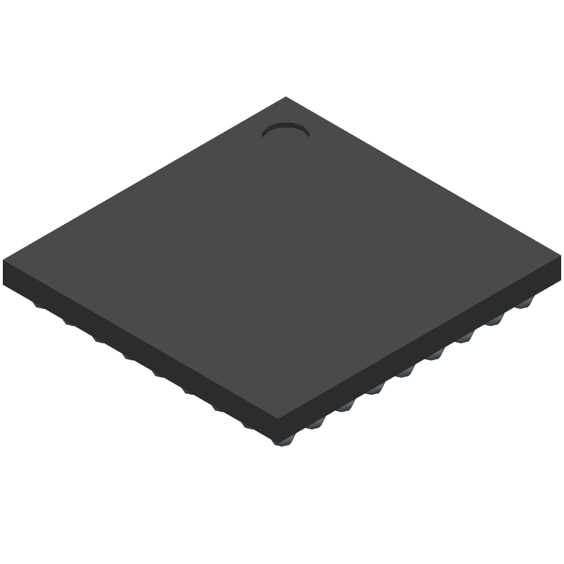
3D Model
Available Download Formats
By downloading CAD models, you agree to our Terms & Conditions and Privacy Policy
Field Programmable Gate Array, 540 CLBs, PBGA81, WLCSP-81
Tip: Data for a part may vary between manufacturers. You can filter for manufacturers on the top of the page next to the part image and part number.
LCMXO3LF-4300E-5UWG81CTR50 by Lattice Semiconductor Corporation is a Field Programmable Gate Array.
Field Programmable Gate Arrays are under the broader part category of Programmable Logic Devices.
Programmable Logic Devices (PLDs) are reconfigurable digital components that can be customized for different applications, offering flexibility and improved performance over fixed logic devices. Read more about Programmable Logic Devices on our Programmable Logic part category page.
| Part # | Distributor | Description | Stock | Price | Buy | |
|---|---|---|---|---|---|---|
|
DISTI #
220-2032-1-ND
|
DigiKey | IC FPGA 63 I/O 81WLCSP Lead time: 16 Weeks Container: Cut Tape (CT), Digi-Reel®, Tape & Reel (TR) | Limited Supply - Call |
|
Buy Now | |
|
|
Vyrian | Programmable ICs | 1583 |
|
RFQ |
By downloading CAD models, you agree to our Terms & Conditions and Privacy Policy
|
|
LCMXO3LF-4300E-5UWG81CTR50
Lattice Semiconductor Corporation
Buy Now
Datasheet
|
Compare Parts:
LCMXO3LF-4300E-5UWG81CTR50
Lattice Semiconductor Corporation
Field Programmable Gate Array, 540 CLBs, PBGA81, WLCSP-81
|
| Rohs Code | Yes | |
| Part Life Cycle Code | Active | |
| Ihs Manufacturer | LATTICE SEMICONDUCTOR CORP | |
| Package Description | WLCSP-81 | |
| Reach Compliance Code | compliant | |
| ECCN Code | EAR99 | |
| HTS Code | 8542.39.00.01 | |
| Samacsys Manufacturer | Lattice Semiconductor | |
| Clock Frequency-Max | 125.9 MHz | |
| JESD-30 Code | R-PBGA-B81 | |
| JESD-609 Code | e1 | |
| Length | 3.797 mm | |
| Moisture Sensitivity Level | 1 | |
| Number of CLBs | 540 | |
| Number of Inputs | 63 | |
| Number of Outputs | 63 | |
| Number of Terminals | 81 | |
| Operating Temperature-Max | 85 °C | |
| Operating Temperature-Min | ||
| Organization | 540 CLBS | |
| Package Body Material | PLASTIC/EPOXY | |
| Package Code | VFBGA | |
| Package Equivalence Code | BGA81,9X9,16 | |
| Package Shape | RECTANGULAR | |
| Package Style | GRID ARRAY, VERY THIN PROFILE, FINE PITCH | |
| Peak Reflow Temperature (Cel) | 260 | |
| Programmable Logic Type | FIELD PROGRAMMABLE GATE ARRAY | |
| Seated Height-Max | 0.567 mm | |
| Supply Voltage-Max | 1.26 V | |
| Supply Voltage-Min | 1.14 V | |
| Supply Voltage-Nom | 1.2 V | |
| Surface Mount | YES | |
| Temperature Grade | OTHER | |
| Terminal Finish | TIN SILVER COPPER | |
| Terminal Form | BALL | |
| Terminal Pitch | 0.4 mm | |
| Terminal Position | BOTTOM | |
| Width | 3.693 mm |
This table gives cross-reference parts and alternative options found for LCMXO3LF-4300E-5UWG81CTR50. The Form Fit Function (FFF) tab will give you the options that are more likely to serve as direct pin-to-pin alternates or drop-in parts. The Functional Equivalents tab will give you options that are likely to match the same function of LCMXO3LF-4300E-5UWG81CTR50, but it may not fit your design. Always verify details of parts you are evaluating, as these parts are offered as suggestions for what you are looking for and are not guaranteed.
| Part Number | Manufacturer | Composite Price | Description | Compare |
|---|---|---|---|---|
| LCMXO3LF-4300E-5UWG81CTR1K | Lattice Semiconductor Corporation | $8.8150 | Field Programmable Gate Array, 540 CLBs, PBGA81, WLCSP-81 | LCMXO3LF-4300E-5UWG81CTR50 vs LCMXO3LF-4300E-5UWG81CTR1K |
Lattice provides a PCB layout guide and reference design files for the LCMXO3LF-4300E-5UWG81CTR50. It's recommended to follow the guidelines for signal integrity, power distribution, and thermal management to ensure optimal performance.
Lattice provides a Secure Enclave IP core and a Secure Boot solution for the LCMXO3LF-4300E-5UWG81CTR50. Engineers can use these resources to implement secure boot and firmware encryption, ensuring the integrity and confidentiality of their design.
The LCMXO3LF-4300E-5UWG81CTR50 has a thermal design power (TDP) of 1.5W. Engineers should ensure proper thermal management by providing adequate heat dissipation, using thermal interfaces, and following Lattice's thermal design guidelines.
Engineers can optimize power consumption by using the device's power-saving features, such as dynamic voltage and frequency scaling, and by implementing power gating and clock gating. Additionally, using a well-designed power distribution network and decoupling capacitors can help reduce power noise.
The LCMXO3LF-4300E-5UWG81CTR50 is not specifically designed for radiation-hardened or high-reliability applications. However, engineers can take measures to mitigate EMI by following proper PCB design and layout practices, using shielding, and implementing EMI filtering.