-
Part Symbol
-
Footprint
-
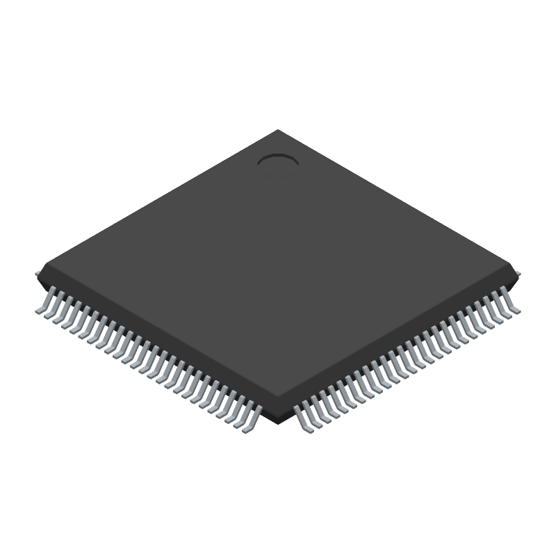
3D Model
Available Download Formats
By downloading CAD models, you agree to our Terms & Conditions and Privacy Policy

Flash PLD, 5.1ns, CMOS, PQFP100, 14 X 14 MM, ROHS COMPLIANT, TQFP-100
Tip: Data for a part may vary between manufacturers. You can filter for manufacturers on the top of the page next to the part image and part number.
LCMXO1200C-3TN100C by Lattice Semiconductor Corporation is a Programmable Logic Device.
Programmable Logic Devices are under the broader part category of Programmable Logic Devices.
Programmable Logic Devices (PLDs) are reconfigurable digital components that can be customized for different applications, offering flexibility and improved performance over fixed logic devices. Read more about Programmable Logic Devices on our Programmable Logic part category page.
| Part # | Distributor | Description | Stock | Price | Buy | |
|---|---|---|---|---|---|---|
|
DISTI #
48W6047
|
Newark | Fpga, 1200 Logic Cell, Tqfp-100, 85Deg C, Fpga Type:Sram Based Fpga, No. Of Logic Cells:1200Logic Cells, Ic Case/Package:Tqfp, No. Of Pins:100Pins, Speed Grade:3, No.of User I/Os:73I/O S, Process Technology:-, Product Range:- Rohs Compliant: Yes |Lattice Semiconductor LCMXO1200C-3TN100C RoHS: Compliant Min Qty: 1 Package Multiple: 1 Date Code: 0 Container: Bulk | 84 |
|
$19.5000 / $23.2500 | Buy Now |
|
DISTI #
220-1177-ND
|
DigiKey | IC FPGA 73 I/O 100TQFP Min Qty: 1 Lead time: 20 Weeks Container: Tray |
5231 In Stock |
|
$18.7500 / $23.2500 | Buy Now |
|
DISTI #
842-MXO1200C3TN100C
|
Mouser Electronics | FPGA - Field Programmable Gate Array 1200 LUTS 73 I/O RoHS: Compliant | 233 |
|
$19.5000 / $23.2500 | Buy Now |
|
DISTI #
E54:1762_00011711
|
Arrow Electronics | FPGA MachXO Family 1200 Cells 130nm Technology 1.8V/2.5V/3.3V 100-Pin TQFP RoHS: Compliant Min Qty: 90 Package Multiple: 90 Lead time: 20 Weeks Date Code: 2419 | Europe - 1350 |
|
$18.5200 | Buy Now |
|
DISTI #
82789570
|
Verical | FPGA MachXO Family 1200 Cells 130nm Technology 1.8V/2.5V/3.3V 100-Pin TQFP RoHS: Compliant Min Qty: 90 Package Multiple: 90 Date Code: 2419 | Americas - 1350 |
|
$18.5200 | Buy Now |
|
|
Flip Electronics | Stock | 6505 |
|
RFQ |
By downloading CAD models, you agree to our Terms & Conditions and Privacy Policy
|
|
LCMXO1200C-3TN100C
Lattice Semiconductor Corporation
Buy Now
Datasheet
|
Compare Parts:
LCMXO1200C-3TN100C
Lattice Semiconductor Corporation
Flash PLD, 5.1ns, CMOS, PQFP100, 14 X 14 MM, ROHS COMPLIANT, TQFP-100
|
| Pbfree Code | Yes | |
| Rohs Code | Yes | |
| Part Life Cycle Code | Active | |
| Ihs Manufacturer | LATTICE SEMICONDUCTOR CORP | |
| Part Package Code | QFP | |
| Package Description | TQFP-100 | |
| Pin Count | 100 | |
| Reach Compliance Code | compliant | |
| ECCN Code | EAR99 | |
| HTS Code | 8542.39.00.01 | |
| Samacsys Manufacturer | Lattice Semiconductor | |
| Clock Frequency-Max | 129.8 MHz | |
| Combinatorial Delay of a CLB-Max | 5.1 ns | |
| JESD-30 Code | S-PQFP-G100 | |
| JESD-609 Code | e3 | |
| Length | 14 mm | |
| Moisture Sensitivity Level | 3 | |
| Number of CLBs | 150 | |
| Number of Inputs | 73 | |
| Number of Logic Cells | 1200 | |
| Number of Outputs | 73 | |
| Number of Terminals | 100 | |
| Operating Temperature-Max | 85 °C | |
| Operating Temperature-Min | ||
| Organization | 150 CLBS | |
| Package Body Material | PLASTIC/EPOXY | |
| Package Code | LFQFP | |
| Package Equivalence Code | QFP100,.63SQ,20 | |
| Package Shape | SQUARE | |
| Package Style | FLATPACK, LOW PROFILE, FINE PITCH | |
| Peak Reflow Temperature (Cel) | 260 | |
| Programmable Logic Type | FIELD PROGRAMMABLE GATE ARRAY | |
| Qualification Status | Not Qualified | |
| Seated Height-Max | 1.6 mm | |
| Supply Voltage-Max | 3.465 V | |
| Supply Voltage-Min | 1.71 V | |
| Supply Voltage-Nom | 1.8 V | |
| Surface Mount | YES | |
| Temperature Grade | OTHER | |
| Terminal Finish | MATTE TIN | |
| Terminal Form | GULL WING | |
| Terminal Pitch | 0.5 mm | |
| Terminal Position | QUAD | |
| Time@Peak Reflow Temperature-Max (s) | 40 | |
| Width | 14 mm |
Lattice Semiconductor provides a PCB layout guide and routing recommendations in their documentation, including the 'Lattice FPGA PCB Design and Layout Guidelines' document. It's essential to follow these guidelines to ensure optimal performance, signal integrity, and thermal management.
A recommended power-up sequence involves a controlled ramp-up of the power supply voltage, followed by a delay to allow the FPGA to stabilize. The 'Lattice FPGA Hardware Checklist' document provides a detailed power-up sequence guideline. Additionally, consider using a power management IC (PMIC) to ensure a clean and stable power supply.
To ensure reliable operation, it's crucial to manage heat dissipation effectively. Use a heat sink or thermal interface material, and ensure good airflow around the FPGA. The 'Lattice FPGA Thermal Management' document provides guidelines for thermal design and management. Consider using a thermal simulation tool to optimize your design.
The LCMXO1200C-3TN100C has a flexible clocking architecture. To optimize clocking, use the Lattice Diamond software to analyze and optimize your clock tree. Consider using a clock domain crossing (CDC) technique to ensure reliable data transfer between clock domains.
The LCMXO1200C-3TN100C has built-in security features, including a secure boot mechanism, AES encryption, and a unique device identifier. Lattice provides a 'Security User Guide' document that outlines the implementation of these features. Additionally, consider using the Lattice Secure Envelope to protect your IP and ensure secure data transmission.