-
Part Symbol
-
Footprint
-
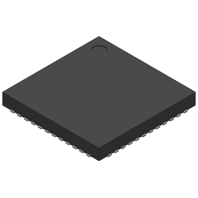
3D Model
Available Download Formats
By downloading CAD models, you agree to our Terms & Conditions and Privacy Policy
Low Power 10-Bit, 250MSPS ADC, QFN, /Tray
Tip: Data for a part may vary between manufacturers. You can filter for manufacturers on the top of the page next to the part image and part number.
KAD5510P-25Q48 by Renesas Electronics Corporation is an Analog to Digital Converter.
Analog to Digital Converters are under the broader part category of Converters.
A converter is an electrical circuit that transforms electric energy into a different form that will support a elecrical load needed by a device. Read more about Converters on our Converters part category page.
| Part # | Distributor | Description | Stock | Price | Buy | |
|---|---|---|---|---|---|---|
|
DISTI #
22T2075
|
Newark | Analog To Digital Converter Adc, 10 Bit, Resolution (Bits):10Bit, Sampling Rate:250Msps, Input Channel Type:Differential, Data Interface:Spi, Supply Voltage Type:Single, Supply Voltage Min:1.7V, Supply Voltage Max:1.9V, Msl:- Rohs Compliant: Yes |Renesas KAD5510P-25Q48 RoHS: Compliant Min Qty: 260 Package Multiple: 1 Date Code: 0 Container: Bulk | 0 |
|
Buy Now | |
|
DISTI #
KAD5510P-25Q48
|
Avnet Silica | Analog to Digital Converter 10 bit Pipelined 250 MSPS Differential 17 V to 19 V 48 Pins QFNEP (Alt: KAD5510P-25Q48) RoHS: Compliant Min Qty: 1 Package Multiple: 1 | Silica - 0 |
|
Buy Now |
By downloading CAD models, you agree to our Terms & Conditions and Privacy Policy
|
|
KAD5510P-25Q48
Renesas Electronics Corporation
Buy Now
Datasheet
|
Compare Parts:
KAD5510P-25Q48
Renesas Electronics Corporation
Low Power 10-Bit, 250MSPS ADC, QFN, /Tray
|
| Pbfree Code | Yes | |
| Rohs Code | Yes | |
| Part Life Cycle Code | Obsolete | |
| Ihs Manufacturer | RENESAS ELECTRONICS CORP | |
| Part Package Code | QFN | |
| Package Description | QFN-48 | |
| Pin Count | 48 | |
| Manufacturer Package Code | L48.7X7E | |
| Reach Compliance Code | compliant | |
| ECCN Code | 3A991.C.1 | |
| HTS Code | 8542.39.00.01 | |
| Samacsys Manufacturer | Renesas Electronics | |
| Analog Input Voltage-Max | 1.54 V | |
| Analog Input Voltage-Min | -1.54 V | |
| Conversion Time-Max | 0.004 µs | |
| Converter Type | ADC, SUCCESSIVE APPROXIMATION | |
| JESD-30 Code | S-PQCC-N48 | |
| JESD-609 Code | e3 | |
| Length | 7 mm | |
| Linearity Error-Max (EL) | 0.0732% | |
| Moisture Sensitivity Level | 3 | |
| Number of Analog In Channels | 1 | |
| Number of Bits | 10 | |
| Number of Functions | 1 | |
| Number of Terminals | 48 | |
| Operating Temperature-Max | 85 °C | |
| Operating Temperature-Min | -40 °C | |
| Output Bit Code | OFFSET BINARY, 2'S COMPLEMENT BINARY, GRAY CODE | |
| Output Format | PARALLEL, WORD | |
| Package Body Material | PLASTIC/EPOXY | |
| Package Code | HVQCCN | |
| Package Equivalence Code | LCC48,.27SQ,20 | |
| Package Shape | SQUARE | |
| Package Style | CHIP CARRIER, HEAT SINK/SLUG, VERY THIN PROFILE | |
| Peak Reflow Temperature (Cel) | 260 | |
| Sample Rate | 250 MHz | |
| Sample and Hold / Track and Hold | SAMPLE | |
| Seated Height-Max | 0.9 mm | |
| Supply Voltage-Nom | 1.8 V | |
| Surface Mount | YES | |
| Technology | CMOS | |
| Temperature Grade | INDUSTRIAL | |
| Terminal Finish | Matte Tin (Sn) - annealed | |
| Terminal Form | NO LEAD | |
| Terminal Pitch | 0.5 mm | |
| Terminal Position | QUAD | |
| Time@Peak Reflow Temperature-Max (s) | 30 | |
| Width | 7 mm |
A 4-layer PCB with a solid ground plane and thermal vias is recommended. The device should be placed near a thermal pad or heat sink to dissipate heat efficiently.
Ensure that the device is operated within the recommended voltage and current ranges, and that the PCB is designed to minimize thermal gradients. Also, consider using thermal protection circuits and over-temperature shutdown mechanisms.
Use high-frequency, low-ESR capacitors (e.g., 0.1uF, 10nF) placed close to the device's power pins. The capacitors should be rated for the maximum operating voltage and have a low inductance to minimize noise and ringing.
Use a shielded enclosure, and ensure that the PCB is designed with EMI-reducing features such as ground planes, guard rings, and signal routing. Also, consider using EMI filters and shielding components.
Route clock signals as differential pairs, using matched impedance and length to minimize skew and jitter. Avoid routing clock signals near noisy signals or power planes.