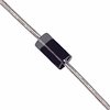
Part Details for JANS1N5418 by Microsemi Corporation
Results Overview of JANS1N5418 by Microsemi Corporation
- Distributor Offerings: (1 listing)
- Number of FFF Equivalents: (2 replacements)
- CAD Models: (Request Part)
- Number of Functional Equivalents: (10 options)
- Part Data Attributes: (Available)
- Reference Designs: (Not Available)
Tip: Data for a part may vary between manufacturers. You can filter for manufacturers on the top of the page next to the part image and part number.
JANS1N5418 Information
JANS1N5418 by Microsemi Corporation is a Rectifier Diode.
Rectifier Diodes are under the broader part category of Diodes.
A diode is a electrical part that can control the direction in which the current flows in a device. Consider factors like voltage drop, current capacity, reverse voltage, and operating frequency when selecting a diode. Read more about Diodes on our Diodes part category page.
Price & Stock for JANS1N5418
| Part # | Distributor | Description | Stock | Price | Buy | |
|---|---|---|---|---|---|---|
|
|
Quest Components | RECTIFIER DIODE,400V V(RRM),SOD-61H2 | 21 |
|
$57.1200 / $67.2000 | Buy Now |
Part Details for JANS1N5418
JANS1N5418 CAD Models
JANS1N5418 Part Data Attributes
|
|
JANS1N5418
Microsemi Corporation
Buy Now
Datasheet
|
Compare Parts:
JANS1N5418
Microsemi Corporation
Rectifier Diode, 1 Phase, 1 Element, 3A, Silicon, SIMILAR TO DO-41, 2 PIN
|
| Rohs Code | No | |
| Part Life Cycle Code | Transferred | |
| Ihs Manufacturer | MICROSEMI CORP | |
| Part Package Code | DO-41 | |
| Package Description | SIMILAR TO DO-41, 2 PIN | |
| Pin Count | 2 | |
| Reach Compliance Code | not_compliant | |
| ECCN Code | EAR99 | |
| HTS Code | 8541.10.00.80 | |
| Samacsys Manufacturer | Microsemi Corporation | |
| Application | FAST RECOVERY POWER | |
| Case Connection | ISOLATED | |
| Configuration | SINGLE | |
| Diode Element Material | SILICON | |
| Diode Type | RECTIFIER DIODE | |
| JESD-30 Code | O-XALF-W2 | |
| JESD-609 Code | e0 | |
| Non-rep Pk Forward Current-Max | 80 A | |
| Number of Elements | 1 | |
| Number of Phases | 1 | |
| Number of Terminals | 2 | |
| Output Current-Max | 3 A | |
| Package Body Material | UNSPECIFIED | |
| Package Shape | ROUND | |
| Package Style | LONG FORM | |
| Qualification Status | Not Qualified | |
| Reference Standard | MIL-19500/411L | |
| Rep Pk Reverse Voltage-Max | 400 V | |
| Reverse Recovery Time-Max | 0.15 µs | |
| Surface Mount | NO | |
| Terminal Finish | Tin/Lead (Sn/Pb) | |
| Terminal Form | WIRE | |
| Terminal Position | AXIAL |
Alternate Parts for JANS1N5418
This table gives cross-reference parts and alternative options found for JANS1N5418. The Form Fit Function (FFF) tab will give you the options that are more likely to serve as direct pin-to-pin alternates or drop-in parts. The Functional Equivalents tab will give you options that are likely to match the same function of JANS1N5418, but it may not fit your design. Always verify details of parts you are evaluating, as these parts are offered as suggestions for what you are looking for and are not guaranteed.
| Part Number | Manufacturer | Composite Price | Description | Compare |
|---|---|---|---|---|
| JAN1N5418 | Microchip Technology Inc | $5.9166 | Rectifier Diode, 1 Phase, 1 Element, 3A, 400V V(RRM), Silicon | JANS1N5418 vs JAN1N5418 |
| 1N5418 | Digitron Semiconductors | Check for Price | Rectifier, Fast Recovery; Max Peak Repetitive Reverse Voltage: 3; Max TMS Bridge Input Voltage: 400; Max DC Reverse Voltage: 1; Package: DIGI-B | JANS1N5418 vs 1N5418 |
JANS1N5418 Frequently Asked Questions (FAQ)
-
The recommended mounting pad layout for the JANS1N5418 is a rectangular pad with a minimum size of 0.05 inches x 0.05 inches (1.27 mm x 1.27 mm) and a maximum size of 0.1 inches x 0.1 inches (2.54 mm x 2.54 mm). The pad should be centered on the device and have a non-solder-mask-defined (NSMD) pad shape.
-
The JANS1N5418 is a sensitive device and requires proper ESD protection during handling and assembly. It is recommended to use an ESD wrist strap or mat, and to handle the device by the body or leads, rather than the glass diode. Additionally, the device should be stored in an ESD-protective package or bag when not in use.
-
The maximum allowable voltage derating for the JANS1N5418 is 10% of the rated voltage. This means that if the device is rated for 100V, the maximum allowable voltage derating would be 10V. Exceeding this derating may affect the device's reliability and performance.
-
Yes, the JANS1N5418 can be used in a switching power supply application, but it is essential to ensure that the device is properly snubbed to prevent voltage spikes and ringing. A snubber circuit can be used to reduce the voltage stress on the device and prevent premature failure.
-
The JANS1N5418 has a cathode (K) and an anode (A) marked on the device. The cathode is the negative terminal, and the anode is the positive terminal. The device should be connected with the correct polarity to ensure proper operation and prevent damage.
