-
Part Symbol
-
Footprint
-
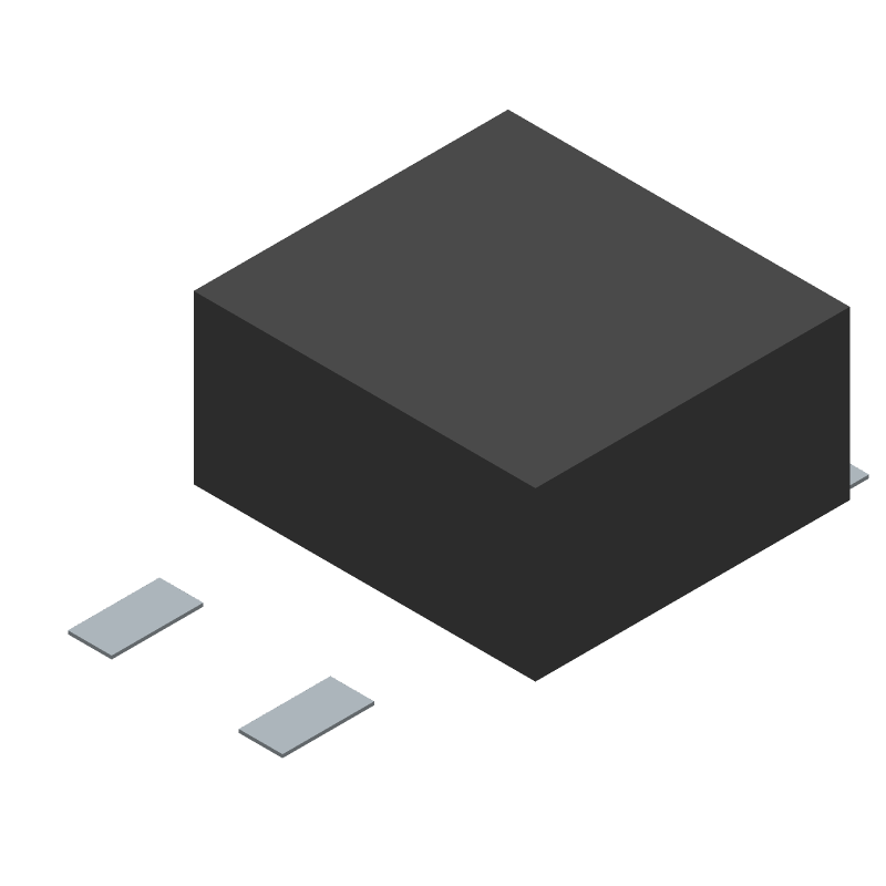
3D Model
Available Download Formats
By downloading CAD models, you agree to our Terms & Conditions and Privacy Policy
Power Field-Effect Transistor,
Tip: Data for a part may vary between manufacturers. You can filter for manufacturers on the top of the page next to the part image and part number.
IXTA08N100D2HV by Littelfuse Inc is a Power Field-Effect Transistor.
Power Field-Effect Transistors are under the broader part category of Transistors.
A transistor is a small semiconductor device used to amplify, control, or create electrical signals. When selecting a transistor, factors such as voltage, current rating, gain, and power dissipation must be considered, with common types. Read more about Transistors on our Transistors part category page.
| Part # | Distributor | Description | Stock | Price | Buy | |
|---|---|---|---|---|---|---|
|
DISTI #
29AK0454
|
Newark | Mosfet, 0.8A, 1Kv, 60W, To-263Hv Rohs Compliant: Yes |Littelfuse IXTA08N100D2HV RoHS: Compliant Min Qty: 1 Package Multiple: 1 Date Code: 1 Container: Bulk | 0 |
|
$2.5800 / $4.2200 | Buy Now |
|
DISTI #
IXTA08N100D2HV-ND
|
DigiKey | MOSFET N-CH 1000V 800MA TO263HV Min Qty: 1 Lead time: 50 Weeks Container: Tube | Temporarily Out of Stock |
|
$2.0101 / $5.3600 | Buy Now |
By downloading CAD models, you agree to our Terms & Conditions and Privacy Policy
|
|
IXTA08N100D2HV
Littelfuse Inc
Buy Now
Datasheet
|
Compare Parts:
IXTA08N100D2HV
Littelfuse Inc
Power Field-Effect Transistor,
|
| Rohs Code | Yes | |
| Part Life Cycle Code | Active | |
| Ihs Manufacturer | LITTELFUSE INC | |
| Package Description | TO-263HV, 2 PIN | |
| Reach Compliance Code | not_compliant | |
| ECCN Code | EAR99 | |
| Samacsys Manufacturer | LITTELFUSE | |
| Case Connection | DRAIN | |
| Configuration | SINGLE WITH BUILT-IN DIODE | |
| Drain-source On Resistance-Max | 21 Ω | |
| FET Technology | METAL-OXIDE SEMICONDUCTOR | |
| Feedback Cap-Max (Crss) | 6.5 pF | |
| JEDEC-95 Code | TO-263AB | |
| JESD-30 Code | R-PSSO-G2 | |
| JESD-609 Code | e3 | |
| Moisture Sensitivity Level | 1 | |
| Number of Elements | 1 | |
| Number of Terminals | 2 | |
| Operating Mode | DEPLETION MODE | |
| Operating Temperature-Max | 150 °C | |
| Operating Temperature-Min | -55 °C | |
| Package Body Material | PLASTIC/EPOXY | |
| Package Shape | RECTANGULAR | |
| Package Style | SMALL OUTLINE | |
| Peak Reflow Temperature (Cel) | 260 | |
| Polarity/Channel Type | N-CHANNEL | |
| Power Dissipation-Max (Abs) | 60 W | |
| Surface Mount | YES | |
| Terminal Finish | Matte Tin (Sn) | |
| Terminal Form | GULL WING | |
| Terminal Position | SINGLE | |
| Time@Peak Reflow Temperature-Max (s) | 10 | |
| Transistor Application | SWITCHING | |
| Transistor Element Material | SILICON |
The recommended PCB footprint for IXTA08N100D2HV is a standard TO-220 package with a minimum pad size of 3.5mm x 2.5mm and a thermal pad size of 2.5mm x 2.5mm.
Yes, IXTA08N100D2HV is suitable for high-frequency switching applications up to 100 kHz, but it's essential to consider the device's switching losses, thermal performance, and layout to ensure reliable operation.
To ensure reliability in high-temperature environments, it's crucial to follow proper thermal management practices, such as providing adequate heat sinking, using a thermal interface material, and keeping the device within its recommended operating temperature range.
Yes, you can parallel multiple IXTA08N100D2HV devices to increase current handling, but it's essential to ensure that the devices are properly matched, and the layout is designed to minimize current imbalance and thermal gradients.
The recommended gate drive voltage for IXTA08N100D2HV is between 10V and 15V, with a maximum gate-source voltage of 20V.