-
Part Symbol
-
Footprint
-
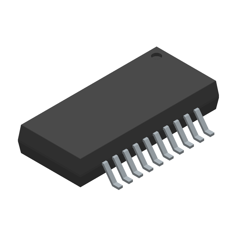
3D Model
Available Download Formats
By downloading CAD models, you agree to our Terms & Conditions and Privacy Policy
Active Clamp Forward PWM Controller, QSOP, /Reel
Tip: Data for a part may vary between manufacturers. You can filter for manufacturers on the top of the page next to the part image and part number.
ISL6726AAZ-T by Renesas Electronics Corporation is a Switching Regulator or Controller.
Switching Regulator or Controllers are under the broader part category of Power Circuits.
A power circuit delivers electricity in order to operate a load for an electronic device. Power circuits include transformers, generators and switches. Read more about Power Circuits on our Power Circuits part category page.
| Part # | Distributor | Description | Stock | Price | Buy | |
|---|---|---|---|---|---|---|
|
DISTI #
20-ISL6726AAZ-TCT-ND
|
DigiKey | IC REG CTRLR MULT TOP 20QSOP Min Qty: 1 Lead time: 18 Weeks Container: Digi-Reel®, Cut Tape (CT), Tape & Reel (TR) |
2490 In Stock |
|
$3.5125 / $8.2200 | Buy Now |
|
DISTI #
ISL6726AAZ-T
|
Avnet Silica | Current Mode PWM Controller 1A 20Pin QSOP TR (Alt: ISL6726AAZ-T) RoHS: Compliant Min Qty: 2500 Package Multiple: 2500 Lead time: 20 Weeks, 0 Days | Silica - 0 |
|
Buy Now | |
|
|
Cytech Systems Limited | IC REG CTRLR MULT TOP 20QSOP | 2500 |
|
RFQ |
By downloading CAD models, you agree to our Terms & Conditions and Privacy Policy
|
|
ISL6726AAZ-T
Renesas Electronics Corporation
Buy Now
Datasheet
|
Compare Parts:
ISL6726AAZ-T
Renesas Electronics Corporation
Active Clamp Forward PWM Controller, QSOP, /Reel
|
| Pbfree Code | Yes | |
| Rohs Code | Yes | |
| Part Life Cycle Code | End Of Life | |
| Ihs Manufacturer | RENESAS ELECTRONICS CORP | |
| Part Package Code | QSOP | |
| Pin Count | 20 | |
| Manufacturer Package Code | M20.15 | |
| Reach Compliance Code | compliant | |
| ECCN Code | EAR99 | |
| HTS Code | 8542.39.00.01 | |
| Factory Lead Time | 18 Weeks | |
| Samacsys Manufacturer | Renesas Electronics | |
| Analog IC - Other Type | SWITCHING CONTROLLER | |
| Control Mode | CURRENT-MODE | |
| Control Technique | PULSE WIDTH MODULATION | |
| Input Voltage-Max | 16 V | |
| Input Voltage-Min | 9 V | |
| Input Voltage-Nom | 12 V | |
| JESD-30 Code | R-PDSO-G20 | |
| JESD-609 Code | e3 | |
| Length | 8.65 mm | |
| Moisture Sensitivity Level | 1 | |
| Number of Functions | 1 | |
| Number of Terminals | 20 | |
| Operating Temperature-Max | 105 °C | |
| Operating Temperature-Min | -40 °C | |
| Output Current-Max | 3 A | |
| Package Body Material | PLASTIC/EPOXY | |
| Package Code | SSOP | |
| Package Shape | RECTANGULAR | |
| Package Style | SMALL OUTLINE, SHRINK PITCH | |
| Peak Reflow Temperature (Cel) | 260 | |
| Seated Height-Max | 1.75 mm | |
| Surface Mount | YES | |
| Switcher Configuration | PHASE-SHIFT | |
| Switching Frequency-Max | 2000 kHz | |
| Technology | BICMOS | |
| Temperature Grade | INDUSTRIAL | |
| Terminal Finish | MATTE TIN | |
| Terminal Form | GULL WING | |
| Terminal Pitch | 0.635 mm | |
| Terminal Position | DUAL | |
| Time@Peak Reflow Temperature-Max (s) | 30 | |
| Width | 3.9 mm |
A good PCB layout for the ISL6726AAZ-T should prioritize thermal management, noise reduction, and signal integrity. Keep the switching node (SW) away from sensitive analog nodes, and use a solid ground plane to reduce EMI. Place the input and output capacitors close to the IC, and use short, wide traces for the power paths.
Choose input capacitors with low ESR and high ripple current ratings to handle the input voltage ripple. For output capacitors, select ones with low ESR, high capacitance, and a voltage rating that exceeds the output voltage. The datasheet recommends a minimum of 10uF for the input capacitor and 22uF for the output capacitor.
The maximum ambient temperature for the ISL6726AAZ-T is 85°C. As the ambient temperature increases, the device's performance may degrade, including reduced efficiency, increased output voltage ripple, and decreased output current capability. Ensure proper thermal management and heat sinking to maintain optimal performance.
The ISL6726AAZ-T has a built-in overcurrent protection feature that can be enabled by connecting the OCP pin to a resistor divider network. The OCP threshold can be set by selecting the appropriate resistor values. The device will shut down if the output current exceeds the set threshold.
The recommended startup sequence is to first apply the input voltage, followed by the enable signal (EN). This ensures that the internal bias voltage is established before the device starts switching. Avoid applying the enable signal before the input voltage, as this can cause damage or malfunction.