-
Part Symbol
-
Footprint
-
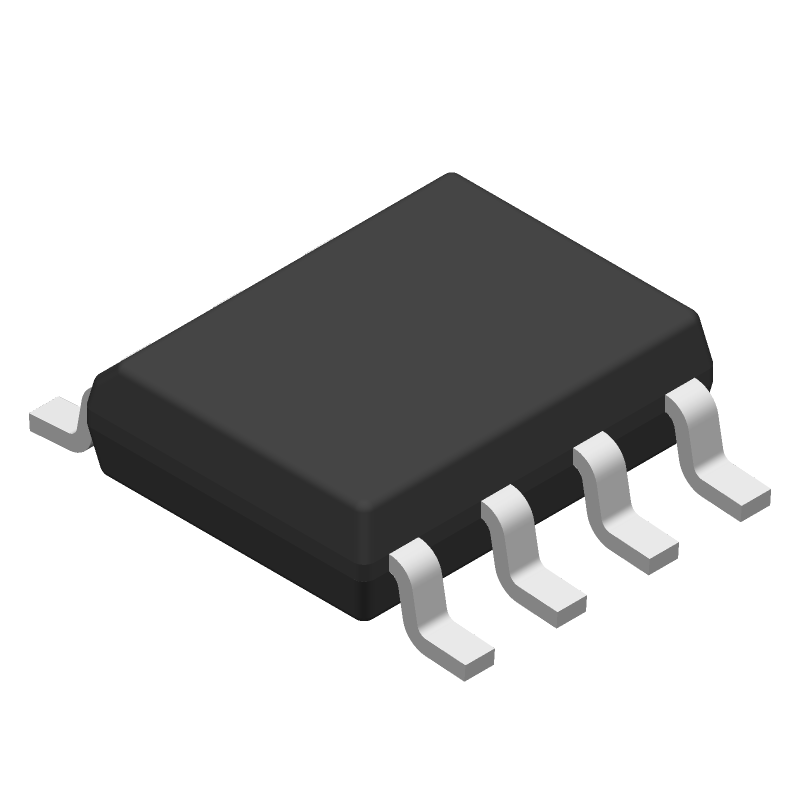
3D Model
Available Download Formats
By downloading CAD models, you agree to our Terms & Conditions and Privacy Policy

Automotive 5-V CAN Transceiver with I/O Level Adapting and Low-Power Mode Supply Optimization 8-SOIC -40 to 125
Tip: Data for a part may vary between manufacturers. You can filter for manufacturers on the top of the page next to the part image and part number.
HVDA553QDRQ1 by Texas Instruments is a Network Interface.
Network Interfaces are under the broader part category of Telecommunication Circuits.
A telecommunications circuit transmits and receives information between points. Key components include transmitters, receivers, amplifiers, and multiplexers. Read more about Telecommunication Circuits on our Telecommunication Circuits part category page.
| Part # | Distributor | Description | Stock | Price | Buy | |
|---|---|---|---|---|---|---|
|
DISTI #
296-40117-1-ND
|
DigiKey | IC TRANSCEIVER HALF 1/2 8SOIC Min Qty: 1 Lead time: 6 Weeks Container: Digi-Reel®, Cut Tape (CT), Tape & Reel (TR) | Temporarily Out of Stock |
|
$1.4668 / $2.6100 | Buy Now |
|
DISTI #
595-HVDA553QDRQ1
|
Mouser Electronics | CAN Interface IC Auto 5V CAN Xcvr RoHS: Compliant | 2471 |
|
$1.4100 / $2.6300 | Buy Now |
|
|
Cytech Systems Limited | IC TRANSCEIVER HALF 1/1 8SOIC | 2500 |
|
RFQ |
By downloading CAD models, you agree to our Terms & Conditions and Privacy Policy
|
|
HVDA553QDRQ1
Texas Instruments
Buy Now
Datasheet
|
Compare Parts:
HVDA553QDRQ1
Texas Instruments
Automotive 5-V CAN Transceiver with I/O Level Adapting and Low-Power Mode Supply Optimization 8-SOIC -40 to 125
|
| Pbfree Code | Yes | |
| Rohs Code | Yes | |
| Part Life Cycle Code | Active | |
| Ihs Manufacturer | TEXAS INSTRUMENTS INC | |
| Package Description | SOIC-8 | |
| Reach Compliance Code | compliant | |
| ECCN Code | EAR99 | |
| HTS Code | 8542.39.00.01 | |
| Samacsys Manufacturer | Texas Instruments | |
| Data Rate | 1000 Mbps | |
| JESD-30 Code | R-PDSO-G8 | |
| JESD-609 Code | e4 | |
| Length | 4.9 mm | |
| Moisture Sensitivity Level | 1 | |
| Number of Channels | 1 | |
| Number of Functions | 1 | |
| Number of Terminals | 8 | |
| Number of Transceivers | 1 | |
| Operating Temperature-Max | 125 °C | |
| Operating Temperature-Min | -40 °C | |
| Package Body Material | PLASTIC/EPOXY | |
| Package Code | SOP | |
| Package Shape | RECTANGULAR | |
| Package Style | SMALL OUTLINE | |
| Peak Reflow Temperature (Cel) | 260 | |
| Screening Level | AEC-Q100 | |
| Seated Height-Max | 1.75 mm | |
| Supply Voltage-Nom | 5 V | |
| Surface Mount | YES | |
| Telecom IC Type | INTERFACE CIRCUIT | |
| Temperature Grade | AUTOMOTIVE | |
| Terminal Finish | Nickel/Palladium/Gold (Ni/Pd/Au) | |
| Terminal Form | GULL WING | |
| Terminal Pitch | 1.27 mm | |
| Terminal Position | DUAL | |
| Time@Peak Reflow Temperature-Max (s) | 30 | |
| Width | 3.9 mm |
A 4-layer PCB with a solid ground plane and a separate power plane is recommended. Keep the analog and digital signal traces separate and avoid crossing them over each other.
Ensure proper thermal management by providing adequate heat sinking and airflow. Use a thermal interface material between the device and the heat sink. Follow the recommended operating conditions and derating guidelines.
Use a shielded enclosure and ensure good grounding practices. Keep the device away from high-frequency sources and use EMI filters or shielding on the input/output lines if necessary.
Use a high-voltage-rated capacitor and resistor in series to limit the voltage and current on the input pins. Ensure the output pins are properly terminated and use a voltage limiter or clamp to prevent overvoltage.
Power up the device in the following sequence: VCC, VDD, and then the input voltage. Power down in the reverse sequence. Ensure a minimum of 10ms delay between power-up and input signal application.