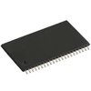
Part Details for HM28100TTI5SE by Renesas Electronics Corporation
Results Overview of HM28100TTI5SE by Renesas Electronics Corporation
- Distributor Offerings: (5 listings)
- Number of FFF Equivalents: (0 replacements)
- CAD Models: (Request Part)
- Number of Functional Equivalents: (0 options)
- Part Data Attributes: (Available)
- Reference Designs: (Not Available)
Tip: Data for a part may vary between manufacturers. You can filter for manufacturers on the top of the page next to the part image and part number.
HM28100TTI5SE Information
HM28100TTI5SE by Renesas Electronics Corporation is an SRAM.
SRAMs are under the broader part category of Memory Components.
Memory components are essential in electronics for computer processing. They can be volatile or non-volatile, depending on the desired function. Read more about Memory Components on our Memory part category page.
Price & Stock for HM28100TTI5SE
| Part # | Distributor | Description | Stock | Price | Buy | |
|---|---|---|---|---|---|---|
|
DISTI #
2156-HM28100TTI5SE-ND
|
DigiKey | IC SRAM 8MBIT PARALLEL 44TSOP II Min Qty: 10 Lead time: 1 Weeks Container: Bulk MARKETPLACE PRODUCT |
86 In Stock |
|
$32.7100 | Buy Now |
|
DISTI #
85989273
|
Verical | Low power SRAM RoHS: Compliant Min Qty: 25 Package Multiple: 1 Date Code: 1901 | Americas - 86 |
|
$31.4500 / $39.3125 | Buy Now |
|
|
Rochester Electronics | HM628100 - 8 M SRAM (1024-K Word X 8-Bit) ' RoHS: Compliant Status: Obsolete Min Qty: 1 | 86 |
|
$25.1600 / $31.4500 | Buy Now |
|
|
GLYN GmbH & Co. KG | SRAM 1Mx8 55nS 5V -40/+85C 44TSOP | 2000 |
|
RFQ | |
|
DISTI #
HM28100TTI5SE
|
Avnet Silica | (Alt: HM28100TTI5SE) RoHS: Compliant Min Qty: 72 Package Multiple: 72 Lead time: 28 Weeks, 0 Days | Silica - 0 |
|
Buy Now |
Part Details for HM28100TTI5SE
HM28100TTI5SE CAD Models
HM28100TTI5SE Part Data Attributes
|
|
HM28100TTI5SE
Renesas Electronics Corporation
Buy Now
Datasheet
|
Compare Parts:
HM28100TTI5SE
Renesas Electronics Corporation
Low Power SRAM, TSOP(2), /Tray
|
| Pbfree Code | Yes | |
| Rohs Code | Yes | |
| Part Life Cycle Code | Obsolete | |
| Ihs Manufacturer | RENESAS ELECTRONICS CORP | |
| Part Package Code | TSOP(2) | |
| Package Description | 0.400 INCH, ROHS COMPLIANT, PLASTIC, TSOP2-44 | |
| Pin Count | 44 | |
| Manufacturer Package Code | PTSB0044GC | |
| Reach Compliance Code | unknown | |
| ECCN Code | 3A991.B.2.A | |
| HTS Code | 8542.32.00.41 | |
| Factory Lead Time | 4 Weeks | |
| Samacsys Manufacturer | Renesas Electronics | |
| Access Time-Max | 55 ns | |
| JESD-30 Code | R-PDSO-G44 | |
| Length | 18.41 mm | |
| Memory Density | 8388608 bit | |
| Memory IC Type | STANDARD SRAM | |
| Memory Width | 8 | |
| Number of Functions | 1 | |
| Number of Terminals | 44 | |
| Number of Words | 1048576 words | |
| Number of Words Code | 1000000 | |
| Operating Mode | ASYNCHRONOUS | |
| Operating Temperature-Max | 85 °C | |
| Operating Temperature-Min | -40 °C | |
| Organization | 1MX8 | |
| Package Body Material | PLASTIC/EPOXY | |
| Package Code | TSOP2 | |
| Package Shape | RECTANGULAR | |
| Package Style | SMALL OUTLINE, THIN PROFILE | |
| Parallel/Serial | PARALLEL | |
| Peak Reflow Temperature (Cel) | NOT SPECIFIED | |
| Seated Height-Max | 1.2 mm | |
| Supply Voltage-Max (Vsup) | 5.5 V | |
| Supply Voltage-Min (Vsup) | 4.5 V | |
| Supply Voltage-Nom (Vsup) | 5 V | |
| Surface Mount | YES | |
| Technology | CMOS | |
| Temperature Grade | INDUSTRIAL | |
| Terminal Form | GULL WING | |
| Terminal Pitch | 0.8 mm | |
| Terminal Position | DUAL | |
| Time@Peak Reflow Temperature-Max (s) | NOT SPECIFIED | |
| Width | 10.16 mm |
HM28100TTI5SE Frequently Asked Questions (FAQ)
-
The recommended power-on sequence is to apply VCC first, followed by VDD, and then the clock signal. This ensures proper initialization of the internal voltage regulators and prevents latch-up.
-
During reset, the JTAG interface should be tri-stated to prevent interference with the reset signal. This can be achieved by setting the JTAG_TMS pin high and the JTAG_TCK pin low.
-
The maximum allowed capacitance on the VCC pin is 10uF. Exceeding this value may cause voltage regulator instability.
-
The HM28100TTI5SE has a built-in watchdog timer that can be enabled by setting the WDTEN bit in the SYSCR register. The watchdog timer can be configured to reset the device or generate an interrupt upon timeout.
-
The maximum frequency for the external clock input is 20MHz. Exceeding this frequency may cause clock signal degradation and affect device operation.
