-
3D Model
Available Download Formats
By downloading CAD models, you agree to our Terms & Conditions and Privacy Policy

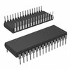
SPECIALTY INTERFACE CIRCUIT, PDIP32, PLASTIC, DIP-32
Tip: Data for a part may vary between manufacturers. You can filter for manufacturers on the top of the page next to the part image and part number.
HCTL-2032 by Avago Technologies is an Other Interface IC.
Other Interface ICs are under the broader part category of Drivers And Interfaces.
A driver controls the current or voltage delivered to components like LCDs or motors, while an interface component connects systems for data transfer and control. Read more about Drivers And Interfaces on our Drivers And Interfaces part category page.
By downloading CAD models, you agree to our Terms & Conditions and Privacy Policy
|
|
HCTL-2032
Avago Technologies
Buy Now
Datasheet
|
Compare Parts:
HCTL-2032
Avago Technologies
SPECIALTY INTERFACE CIRCUIT, PDIP32, PLASTIC, DIP-32
|
| Pbfree Code | Yes | |
| Rohs Code | Yes | |
| Part Life Cycle Code | Obsolete | |
| Ihs Manufacturer | AVAGO TECHNOLOGIES INC | |
| Part Package Code | DIP | |
| Package Description | DIP, DIP32,.6 | |
| Pin Count | 32 | |
| Reach Compliance Code | compliant | |
| HTS Code | 8542.39.00.01 | |
| Samacsys Manufacturer | Avago Technologies | |
| Interface IC Type | INTERFACE CIRCUIT | |
| JESD-30 Code | R-PDIP-T32 | |
| JESD-609 Code | e3 | |
| Length | 41.91 mm | |
| Number of Functions | 1 | |
| Number of Terminals | 32 | |
| Operating Temperature-Max | 100 °C | |
| Operating Temperature-Min | -40 °C | |
| Package Body Material | PLASTIC/EPOXY | |
| Package Code | DIP | |
| Package Equivalence Code | DIP32,.6 | |
| Package Shape | RECTANGULAR | |
| Package Style | IN-LINE | |
| Peak Reflow Temperature (Cel) | 260 | |
| Qualification Status | Not Qualified | |
| Supply Voltage-Max | 5.5 V | |
| Supply Voltage-Min | 4.5 V | |
| Supply Voltage-Nom | 5 V | |
| Surface Mount | NO | |
| Technology | CMOS | |
| Temperature Grade | INDUSTRIAL | |
| Terminal Finish | MATTE TIN | |
| Terminal Form | THROUGH-HOLE | |
| Terminal Pitch | 2.54 mm | |
| Terminal Position | DUAL | |
| Width | 15.24 mm |
A 4-layer PCB with a solid ground plane and a separate power plane is recommended. Keep the signal traces short and away from noise sources. Use a common mode filter or a ferrite bead to reduce EMI.
Use a heat sink or a thermal pad to dissipate heat. Ensure good airflow around the device. Consider using a thermal interface material to improve heat transfer. Operate the device within the recommended temperature range (0°C to 70°C).
Power up the VCC pin first, followed by the VEE pin. Ensure that the VCC pin is powered up before the VEE pin reaches its operating voltage. This prevents latch-up and ensures reliable operation.
Check the clock output frequency and amplitude using an oscilloscope. Verify that the clock input is within the recommended frequency range (25 MHz to 200 MHz). Check for noise or jitter on the clock input. Ensure that the clock output is properly terminated.
Use a 50-ohm transmission line or a controlled impedance PCB trace to drive the output. Use a series resistor (e.g., 22 ohms) to match the output impedance to the transmission line. Ensure that the output is properly terminated to prevent reflections.