-
Part Symbol
-
Footprint
-
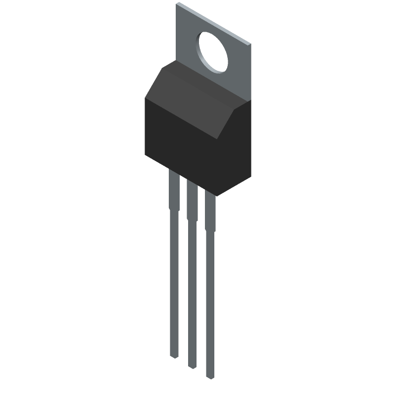
3D Model
Available Download Formats
By downloading CAD models, you agree to our Terms & Conditions and Privacy Policy
Power MOSFET, N-Channel, UniFETTM, 60 V, 65 A, 16 mΩ, TO-220, TO-220-3, 1000-TUBE
Tip: Data for a part may vary between manufacturers. You can filter for manufacturers on the top of the page next to the part image and part number.
FDP65N06 by onsemi is a Power Field-Effect Transistor.
Power Field-Effect Transistors are under the broader part category of Transistors.
A transistor is a small semiconductor device used to amplify, control, or create electrical signals. When selecting a transistor, factors such as voltage, current rating, gain, and power dissipation must be considered, with common types. Read more about Transistors on our Transistors part category page.
| Part # | Distributor | Description | Stock | Price | Buy | |
|---|---|---|---|---|---|---|
|
DISTI #
04M9106
|
Newark | N Channel Mosfet, 60V, 65A, To-220, Channel Type:N Channel, Drain Source Voltage Vds:60V, Continuous Drain Current Id:65A, Transistor Mounting:Through Hole, Rds(On) Test Voltage:10V, Gate Source Threshold Voltage Max:2V, Msl:- Rohs Compliant: Yes |Onsemi FDP65N06 RoHS: Compliant Min Qty: 1000 Package Multiple: 1 Date Code: 0 Container: Bulk | 0 |
|
$0.9070 / $1.1400 | Buy Now |
|
|
Flip Electronics | Stock, ship today | 5545 |
|
RFQ |
By downloading CAD models, you agree to our Terms & Conditions and Privacy Policy
|
|
FDP65N06
onsemi
Buy Now
Datasheet
|
Compare Parts:
FDP65N06
onsemi
Power MOSFET, N-Channel, UniFETTM, 60 V, 65 A, 16 mΩ, TO-220, TO-220-3, 1000-TUBE
|
| Pbfree Code | Yes | |
| Rohs Code | Yes | |
| Part Life Cycle Code | Obsolete | |
| Ihs Manufacturer | ONSEMI | |
| Part Package Code | TO-220-3 | |
| Package Description | TO-220, 3 PIN | |
| Manufacturer Package Code | 340AT | |
| Reach Compliance Code | not_compliant | |
| ECCN Code | EAR99 | |
| Factory Lead Time | 2 Days | |
| Samacsys Manufacturer | onsemi | |
| Avalanche Energy Rating (Eas) | 430 mJ | |
| Configuration | SINGLE WITH BUILT-IN DIODE | |
| DS Breakdown Voltage-Min | 60 V | |
| Drain Current-Max (ID) | 65 A | |
| Drain-source On Resistance-Max | 0.016 Ω | |
| FET Technology | METAL-OXIDE SEMICONDUCTOR | |
| JEDEC-95 Code | TO-220AB | |
| JESD-30 Code | R-PSFM-T3 | |
| JESD-609 Code | e3 | |
| Number of Elements | 1 | |
| Number of Terminals | 3 | |
| Operating Mode | ENHANCEMENT MODE | |
| Operating Temperature-Max | 150 °C | |
| Package Body Material | PLASTIC/EPOXY | |
| Package Shape | RECTANGULAR | |
| Package Style | FLANGE MOUNT | |
| Polarity/Channel Type | N-CHANNEL | |
| Power Dissipation-Max (Abs) | 135 W | |
| Pulsed Drain Current-Max (IDM) | 260 A | |
| Qualification Status | Not Qualified | |
| Surface Mount | NO | |
| Terminal Finish | MATTE TIN | |
| Terminal Form | THROUGH-HOLE | |
| Terminal Position | SINGLE | |
| Transistor Application | SWITCHING | |
| Transistor Element Material | SILICON |
The maximum junction temperature that the FDP65N06 can withstand is 175°C. Exceeding this temperature can lead to device failure.
To ensure proper biasing, the FDP65N06 requires a gate-source voltage (Vgs) between 4V and 10V, and a drain-source voltage (Vds) between 10V and 60V. Additionally, a gate resistor (Rg) between 1kΩ and 10kΩ is recommended to prevent oscillations.
To minimize parasitic inductance and capacitance, it is recommended to use a compact PCB layout with short leads and a solid ground plane. The drain and source pins should be connected to the PCB with minimal lead length, and the gate pin should be connected to a low-impedance signal source.
Yes, the FDP65N06 can be used in high-frequency switching applications up to 1 MHz. However, it is essential to ensure proper PCB layout, decoupling, and gate drive to minimize ringing and oscillations.
To protect the FDP65N06 from ESD, it is recommended to handle the device with an anti-static wrist strap or mat, and to use ESD-protected workstations and tools. Additionally, the device should be stored in an anti-static package or bag when not in use.