-
Part Symbol
-
Footprint
-
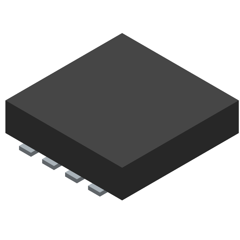
3D Model
Available Download Formats
By downloading CAD models, you agree to our Terms & Conditions and Privacy Policy
30V N-Channel Power Trench® MOSFET, 3000-REEL
Tip: Data for a part may vary between manufacturers. You can filter for manufacturers on the top of the page next to the part image and part number.
FDMC8884 by onsemi is a Power Field-Effect Transistor.
Power Field-Effect Transistors are under the broader part category of Transistors.
A transistor is a small semiconductor device used to amplify, control, or create electrical signals. When selecting a transistor, factors such as voltage, current rating, gain, and power dissipation must be considered, with common types. Read more about Transistors on our Transistors part category page.
| Part # | Distributor | Description | Stock | Price | Buy | |
|---|---|---|---|---|---|---|
|
DISTI #
85983149
|
Verical | Trans MOSFET N-CH Si 30V 9A 8-Pin WDFN EP T/R RoHS: Compliant Min Qty: 871 Package Multiple: 1 Date Code: 1801 | Americas - 23691 |
|
$0.2969 / $0.4310 | Buy Now |
|
|
Rochester Electronics | 9A, 30V, 0.019ohm, N-Channel Power MOSFET RoHS: Compliant Status: Obsolete Min Qty: 1 | 23691 |
|
$0.2375 / $0.3831 | Buy Now |
By downloading CAD models, you agree to our Terms & Conditions and Privacy Policy
|
|
FDMC8884
onsemi
Buy Now
Datasheet
|
Compare Parts:
FDMC8884
onsemi
30V N-Channel Power Trench® MOSFET, 3000-REEL
|
| Pbfree Code | Yes | |
| Rohs Code | Yes | |
| Part Life Cycle Code | Obsolete | |
| Ihs Manufacturer | ONSEMI | |
| Package Description | MO-229, 8 PIN | |
| Manufacturer Package Code | 511DQ | |
| Reach Compliance Code | compliant | |
| ECCN Code | EAR99 | |
| Factory Lead Time | 4 Weeks | |
| Samacsys Manufacturer | onsemi | |
| Avalanche Energy Rating (Eas) | 24 mJ | |
| Case Connection | DRAIN | |
| Configuration | SINGLE WITH BUILT-IN DIODE | |
| DS Breakdown Voltage-Min | 30 V | |
| Drain Current-Max (ID) | 9 A | |
| Drain-source On Resistance-Max | 0.019 Ω | |
| FET Technology | METAL-OXIDE SEMICONDUCTOR | |
| JESD-30 Code | S-PDSO-N5 | |
| JESD-609 Code | e4 | |
| Moisture Sensitivity Level | 1 | |
| Number of Elements | 1 | |
| Number of Terminals | 5 | |
| Operating Mode | ENHANCEMENT MODE | |
| Operating Temperature-Max | 150 °C | |
| Package Body Material | PLASTIC/EPOXY | |
| Package Shape | SQUARE | |
| Package Style | SMALL OUTLINE | |
| Peak Reflow Temperature (Cel) | 260 | |
| Polarity/Channel Type | N-CHANNEL | |
| Power Dissipation-Max (Abs) | 18 W | |
| Pulsed Drain Current-Max (IDM) | 40 A | |
| Qualification Status | Not Qualified | |
| Surface Mount | YES | |
| Terminal Finish | NICKEL PALLADIUM GOLD | |
| Terminal Form | NO LEAD | |
| Terminal Position | DUAL | |
| Time@Peak Reflow Temperature-Max (s) | 30 | |
| Transistor Application | SWITCHING | |
| Transistor Element Material | SILICON |
A 4-layer PCB with a solid ground plane and thermal vias is recommended. Keep the thermal pad connected to the ground plane to improve heat dissipation.
Ensure proper thermal design, use a heat sink if necessary, and follow the recommended operating conditions. Monitor the junction temperature (TJ) and adjust the design accordingly.
The maximum allowed voltage on the input pins is 5.5V. Exceeding this voltage may damage the device.
Use ESD protection devices such as TVS diodes or ESD arrays on the input lines. Follow proper PCB design and handling practices to minimize ESD risks.
Power up the device in the following sequence: VCC, then VDD, and finally the input signals. This ensures proper device initialization and prevents latch-up.