-
Part Symbol
-
Footprint
-
3D Model
Available Download Formats
By downloading CAD models, you agree to our Terms & Conditions and Privacy Policy
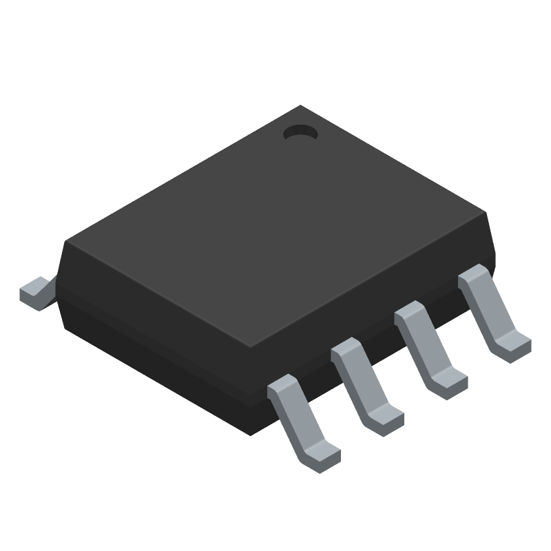
Integrated P-Channel PowerTrench® MOSFET and Schottky Diode -30V, -3A, 115mΩ, SOIC-8, 2500-REEL
Tip: Data for a part may vary between manufacturers. You can filter for manufacturers on the top of the page next to the part image and part number.
FDFS2P753Z by onsemi is a Power Field-Effect Transistor.
Power Field-Effect Transistors are under the broader part category of Transistors.
A transistor is a small semiconductor device used to amplify, control, or create electrical signals. When selecting a transistor, factors such as voltage, current rating, gain, and power dissipation must be considered, with common types. Read more about Transistors on our Transistors part category page.
| Part # | Distributor | Description | Stock | Price | Buy | |
|---|---|---|---|---|---|---|
|
DISTI #
2156-FDFS2P753Z-488-ND
|
DigiKey | POWER FIELD-EFFECT TRANSISTOR, 3 Min Qty: 841 Lead time: 1 Weeks Container: Bulk MARKETPLACE PRODUCT |
5825 In Stock |
|
$0.3600 | Buy Now |
|
DISTI #
V72:2272_06300666
|
Arrow Electronics | Trans MOSFET P-CH 30V 3A 8-Pin SOIC T/R RoHS: Compliant Min Qty: 1 Package Multiple: 1 Lead time: 99 Weeks Date Code: 1931 Container: Cut Strips | Americas - 29 |
|
$0.0349 / $0.0361 | Buy Now |
|
DISTI #
85986635
|
Verical | Trans MOSFET P-CH 30V 3A 8-Pin SOIC T/R RoHS: Compliant Min Qty: 874 Package Multiple: 1 Date Code: 1901 | Americas - 5825 |
|
$0.4293 | Buy Now |
|
|
Rochester Electronics | Power Field-Effect Transistor, 3A, 30V, 0.162ohm, P-Channel, MOSFET RoHS: Compliant Status: Obsolete Min Qty: 1 | 5825 |
|
$0.2129 / $0.3434 | Buy Now |
|
DISTI #
FDFS2P753Z
|
Avnet Silica | Trans MOSFET PCH 30V 3A 8Pin SOIC N TR (Alt: FDFS2P753Z) RoHS: Compliant Min Qty: 2500 Package Multiple: 2500 Lead time: 143 Weeks, 0 Days | Silica - 0 |
|
Buy Now | |
|
DISTI #
FDFS2P753Z
|
EBV Elektronik | Trans MOSFET PCH 30V 3A 8Pin SOIC N TR (Alt: FDFS2P753Z) RoHS: Compliant Min Qty: 2500 Package Multiple: 2500 Lead time: 143 Weeks, 0 Days | EBV - 0 |
|
Buy Now |
By downloading CAD models, you agree to our Terms & Conditions and Privacy Policy
|
|
FDFS2P753Z
onsemi
Buy Now
Datasheet
|
Compare Parts:
FDFS2P753Z
onsemi
Integrated P-Channel PowerTrench® MOSFET and Schottky Diode -30V, -3A, 115mΩ, SOIC-8, 2500-REEL
|
| Pbfree Code | Yes | |
| Rohs Code | Yes | |
| Part Life Cycle Code | Obsolete | |
| Ihs Manufacturer | ONSEMI | |
| Part Package Code | SOIC-8 | |
| Package Description | SO-8 | |
| Manufacturer Package Code | 751EB | |
| Reach Compliance Code | compliant | |
| ECCN Code | EAR99 | |
| Factory Lead Time | 4 Weeks | |
| Samacsys Manufacturer | onsemi | |
| Avalanche Energy Rating (Eas) | 6 mJ | |
| Configuration | SINGLE WITH BUILT-IN DIODE | |
| DS Breakdown Voltage-Min | 30 V | |
| Drain Current-Max (ID) | 3 A | |
| Drain-source On Resistance-Max | 0.162 Ω | |
| FET Technology | METAL-OXIDE SEMICONDUCTOR | |
| JESD-30 Code | R-PDSO-G8 | |
| JESD-609 Code | e3 | |
| Moisture Sensitivity Level | 1 | |
| Number of Elements | 1 | |
| Number of Terminals | 8 | |
| Operating Mode | ENHANCEMENT MODE | |
| Operating Temperature-Max | 150 °C | |
| Package Body Material | PLASTIC/EPOXY | |
| Package Shape | RECTANGULAR | |
| Package Style | SMALL OUTLINE | |
| Peak Reflow Temperature (Cel) | 260 | |
| Polarity/Channel Type | P-CHANNEL | |
| Power Dissipation-Max (Abs) | 1.6 W | |
| Pulsed Drain Current-Max (IDM) | 16 A | |
| Qualification Status | Not Qualified | |
| Surface Mount | YES | |
| Terminal Finish | Tin (Sn) | |
| Terminal Form | GULL WING | |
| Terminal Position | DUAL | |
| Time@Peak Reflow Temperature-Max (s) | 30 | |
| Transistor Element Material | SILICON |
A 2-layer or 4-layer PCB with a solid ground plane and thermal vias is recommended. Ensure a minimum of 1 oz copper thickness and a thermal relief pattern under the device.
Implement a robust thermal management system, including a heat sink, thermal interface material, and a cooling fan if necessary. Monitor the device's junction temperature and adjust the system design accordingly.
Use a reflow soldering process with a peak temperature of 260°C (500°F) and a dwell time of 20-30 seconds. Ensure the device is soldered within the recommended temperature range to prevent damage.
Handle the device in an ESD-controlled environment, use ESD-protective packaging, and ensure all equipment and personnel are grounded. Implement ESD protection circuits in the system design if necessary.
Use a low-ESR ceramic capacitor with a value of 10-22 μF and a voltage rating of 25-50 V. The capacitor should be placed as close as possible to the device's input pins.