-
Part Symbol
-
Footprint
-
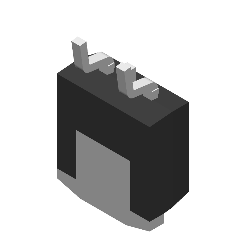
3D Model
Available Download Formats
By downloading CAD models, you agree to our Terms & Conditions and Privacy Policy
N-Channel PowerTrench® MOSFET 40V, 182A, 3mΩ, D2PAK-3 / TO-263-2, 800-REEL
Tip: Data for a part may vary between manufacturers. You can filter for manufacturers on the top of the page next to the part image and part number.
FDB8443 by onsemi is a Power Field-Effect Transistor.
Power Field-Effect Transistors are under the broader part category of Transistors.
A transistor is a small semiconductor device used to amplify, control, or create electrical signals. When selecting a transistor, factors such as voltage, current rating, gain, and power dissipation must be considered, with common types. Read more about Transistors on our Transistors part category page.
| Part # | Distributor | Description | Stock | Price | Buy | |
|---|---|---|---|---|---|---|
|
|
Rochester Electronics | FDB8443 - N-Channel PowerTrench MOSFET 40V, 182A RoHS: Compliant Status: Obsolete Min Qty: 1 | 17600 |
|
$1.5400 / $1.9300 | Buy Now |
|
DISTI #
FDB8443
|
Avnet Silica | Trans MOSFET NCH 40V 25A 3Pin2Tab D2PAK TR (Alt: FDB8443) RoHS: Compliant Min Qty: 800 Package Multiple: 800 Lead time: 143 Weeks, 0 Days | Silica - 0 |
|
Buy Now | |
|
|
Cytech Systems Limited | MOSFET N-CH 40V 25A/120A TO263AB | 1200 |
|
RFQ |
By downloading CAD models, you agree to our Terms & Conditions and Privacy Policy
|
|
FDB8443
onsemi
Buy Now
Datasheet
|
Compare Parts:
FDB8443
onsemi
N-Channel PowerTrench® MOSFET 40V, 182A, 3mΩ, D2PAK-3 / TO-263-2, 800-REEL
|
| Pbfree Code | Yes | |
| Rohs Code | Yes | |
| Part Life Cycle Code | Obsolete | |
| Ihs Manufacturer | ONSEMI | |
| Part Package Code | D2PAK-3 / TO-263-2 | |
| Package Description | ROHS COMPLIANT PACKAGE-3 | |
| Manufacturer Package Code | 418AJ | |
| Reach Compliance Code | not_compliant | |
| ECCN Code | EAR99 | |
| Factory Lead Time | 4 Weeks | |
| Samacsys Manufacturer | onsemi | |
| Avalanche Energy Rating (Eas) | 531 mJ | |
| Case Connection | DRAIN | |
| Configuration | SINGLE WITH BUILT-IN DIODE | |
| DS Breakdown Voltage-Min | 40 V | |
| Drain Current-Max (ID) | 25 A | |
| Drain-source On Resistance-Max | 0.003 Ω | |
| FET Technology | METAL-OXIDE SEMICONDUCTOR | |
| JEDEC-95 Code | TO-263AB | |
| JESD-30 Code | R-PSSO-G2 | |
| JESD-609 Code | e3 | |
| Moisture Sensitivity Level | 1 | |
| Number of Elements | 1 | |
| Number of Terminals | 2 | |
| Operating Mode | ENHANCEMENT MODE | |
| Operating Temperature-Max | 175 °C | |
| Package Body Material | PLASTIC/EPOXY | |
| Package Shape | RECTANGULAR | |
| Package Style | SMALL OUTLINE | |
| Peak Reflow Temperature (Cel) | 245 | |
| Polarity/Channel Type | N-CHANNEL | |
| Power Dissipation-Max (Abs) | 188 W | |
| Qualification Status | Not Qualified | |
| Surface Mount | YES | |
| Terminal Finish | Matte Tin (Sn) - annealed | |
| Terminal Form | GULL WING | |
| Terminal Position | SINGLE | |
| Time@Peak Reflow Temperature-Max (s) | 30 | |
| Transistor Application | SWITCHING | |
| Transistor Element Material | SILICON |
This table gives cross-reference parts and alternative options found for FDB8443. The Form Fit Function (FFF) tab will give you the options that are more likely to serve as direct pin-to-pin alternates or drop-in parts. The Functional Equivalents tab will give you options that are likely to match the same function of FDB8443, but it may not fit your design. Always verify details of parts you are evaluating, as these parts are offered as suggestions for what you are looking for and are not guaranteed.
| Part Number | Manufacturer | Composite Price | Description | Compare |
|---|---|---|---|---|
| FDB8443_F085 | Fairchild Semiconductor Corporation | Check for Price | Power Field-Effect Transistor, 25A I(D), 40V, 0.003ohm, 1-Element, N-Channel, Silicon, Metal-oxide Semiconductor FET, TO-263AB, ROHS COMPLIANT PACKAGE-3 | FDB8443 vs FDB8443_F085 |
A good PCB layout for optimal thermal performance involves placing thermal vias under the FDB8443 package, using a solid ground plane, and keeping the thermal traces as short and wide as possible. A 4-layer PCB with a dedicated thermal layer is also recommended.
To ensure proper biasing, make sure to follow the recommended voltage and current ratings in the datasheet. Also, use a stable voltage source, and decouple the input and output pins with suitable capacitors to minimize noise and oscillations.
Critical parameters to monitor during FDB8443 operation include junction temperature, input and output voltage, current, and power dissipation. Monitoring these parameters can help prevent overheating, overvoltage, and overcurrent conditions that can damage the device.
To protect the FDB8443 from ESD, handle the device with an anti-static wrist strap or mat, and ensure that the PCB is designed with ESD protection in mind, such as using ESD diodes or resistors on the input and output pins.
Recommended soldering and assembly techniques for the FDB8443 include using a soldering iron with a temperature-controlled tip, applying a small amount of solder paste, and using a reflow oven or hot air soldering technique to minimize thermal stress on the device.